VTC4 Просмотр технического описания (PDF) - Vectron International
Номер в каталоге
Компоненты Описание
Список матч
VTC4 Datasheet PDF : 7 Pages
| |||
VTC4 Data Sheet
VCXO Functional Description
VCXO Feature: The VTC4 can be ordered with a VCXO function for applications where it will be used in a
PLL, or the output frequency needs fine tune adjustments. This is a high impedance input, 1 Mohm, and can
be driven with an op-amp or terminated with adjustable resistors etc. Pin 1 should not be left floating on
the VCXO optional devices.
“No Adjust” Feature: In applications where the VTC4 will not be used in a PLL, or the output frequency
does not fine tune adjustments, the best device to use would be a VTC4-x0xx. By using the “no adjust”
option, the circuit is simplified as Vc does not need to adjusted or set to a predetermined voltage and pin 1
should be grounded (pin 1 can be left open but should not be set to a voltage such as the supply).
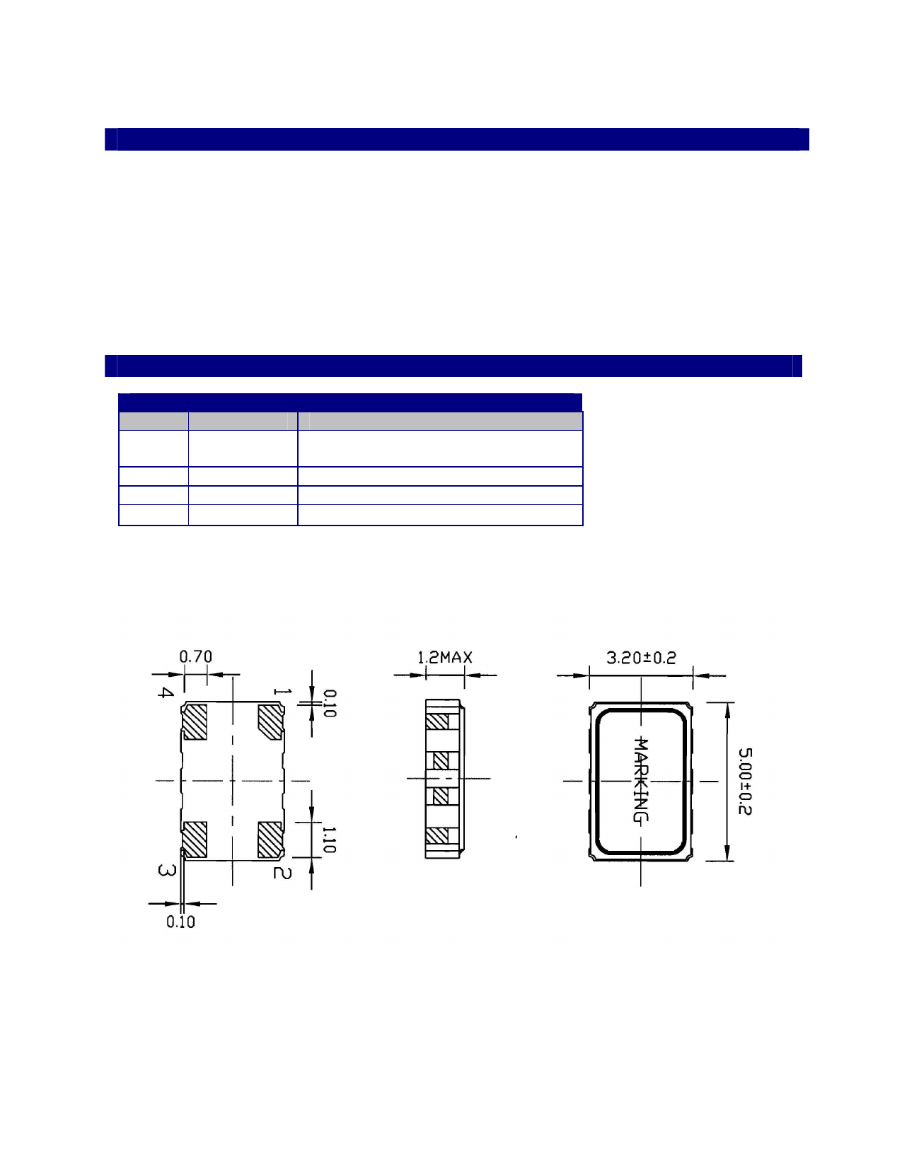
Outline Diagrams, Pad Layout and Pin Out
Table 2. Pinout
Pin #
Symbol
1
GND or
VC
2
GND
3
fO
4
VDD
Function
Ground for a VTC4-x0xx option
or VCXO Control Voltage
Electrical and Case Ground
Output Frequency
Supply Voltage
NOTE: Additional pads are used to program and adjust the TCXO during manufacturing and should be left
open; do not terminate these to the supply voltage. Some designs do not include these additional pads.
Contact Pads are gold over nickel
Devices will be marked with the frequency
Figure 3, Package drawing
Vectron International 267 Lowell Rd, Hudson NH 03051 Tel: 1-88-VECTRON-1 e-mail: vectron@vectron.com
Share Link: 