VOM617A Просмотр технического описания (PDF) - Vishay Semiconductors
Номер в каталоге
Компоненты Описание
Список матч
VOM617A Datasheet PDF : 8 Pages
| |||
www.vishay.com
VOM617A
Vishay Semiconductors
ABSOLUTE MAXIMUM RATINGS (Tamb = 25 °C, unless otherwise specified)
PARAMETER
TEST CONDITION
SYMBOL
VALUE
UNIT
INPUT
DC forward current
Reverse voltage
Power dissipation
Surge forward current
OUTPUT
IF
60
mA
VR
6
V
Pdiss
70
mW
tp ≤ 10 μs
IFSM
2.5
A
Collector emitter voltage
Emitter collector voltage
Collector current
Power dissipation
COUPLER
VCEO
80
V
VECO
7
V
IC
tp ≤ 1 ms
50
mA
100
mA
Pdiss
150
mW
Isolation test voltage
between emitter and detector
t = 1 min
VISO
3750
VRMS
Total power dissipation
Operating temperature range
Storage temperature range
Junction temperature
Soldering temperature (1)
Ptot
170
mW
Tamb
- 55 to + 110
°C
Tstg
- 55 to + 150
°C
Tj
125
°C
Tsld
260
°C
Notes
• Stresses in excess of the absolute maximum ratings can cause permanent damage to the device. Functional operation of the device is not
implied at these or any other conditions in excess of those given in the operational sections of this document. Exposure to absolute
maximum ratings for extended periods of the time can adversely affect reliability.
(1) See “Assembly Instructions” for surface mounted devices (www.vishay.com/doc?80054).
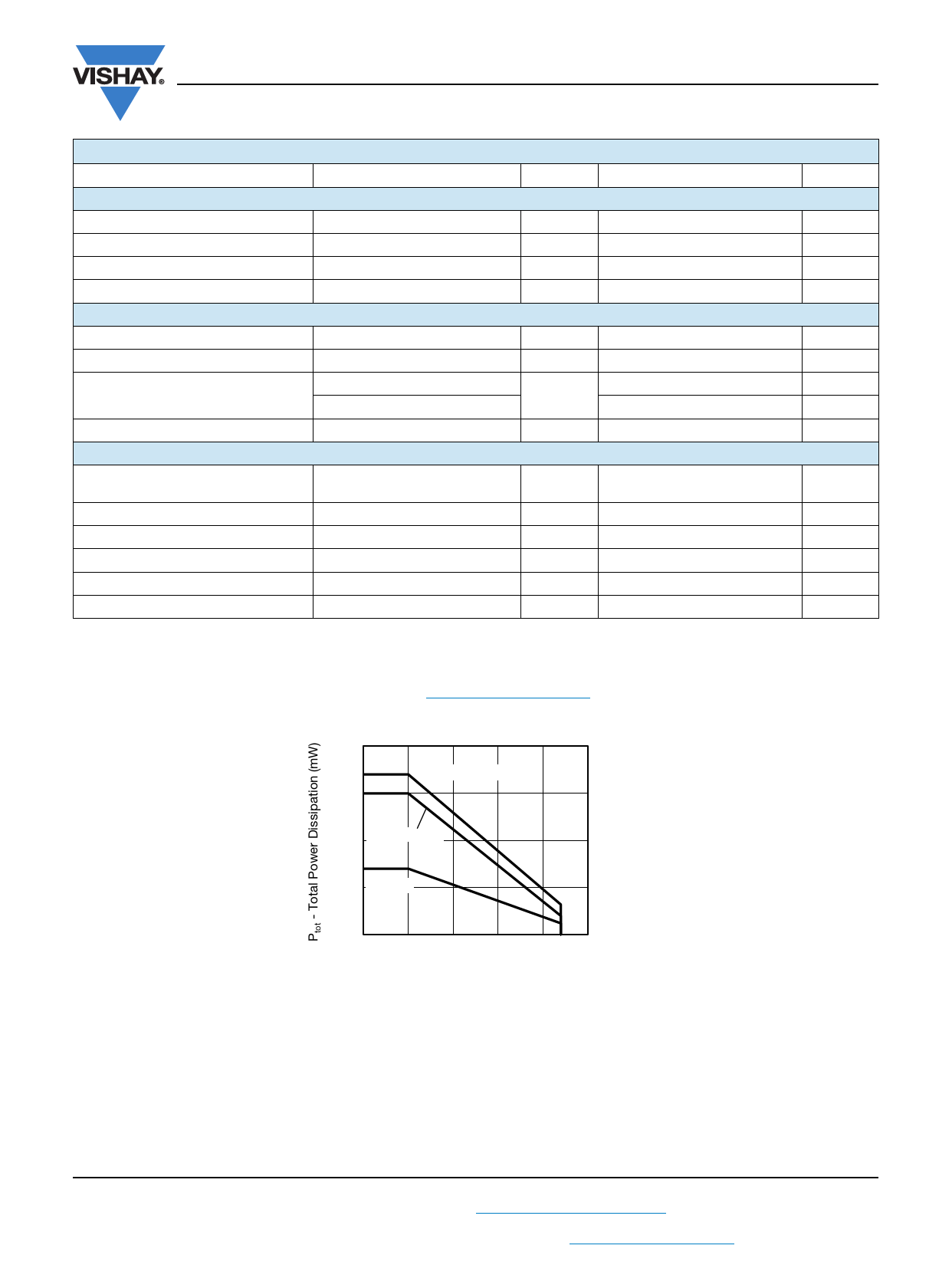
200
Coupled device
150
100 Phototransistor
50 IR-diode
0
0
25
50
75
100 125
Tamb - Ambient Temperature (°C)
Fig. 1 - Total Power Dissipation vs. Ambient Temperature
Rev. 1.3, 11-Dec-12
2
Document Number: 83446
For technical questions, contact: optocoupleranswers@vishay.com
THIS DOCUMENT IS SUBJECT TO CHANGE WITHOUT NOTICE. THE PRODUCTS DESCRIBED HEREIN AND THIS DOCUMENT
ARE SUBJECT TO SPECIFIC DISCLAIMERS, SET FORTH AT www.vishay.com/doc?91000
Share Link: 