GF9102A Просмотр технического описания (PDF) - Gennum -> Semtech
Номер в каталоге
Компоненты Описание
Список матч
GF9102A Datasheet PDF : 11 Pages
| |||
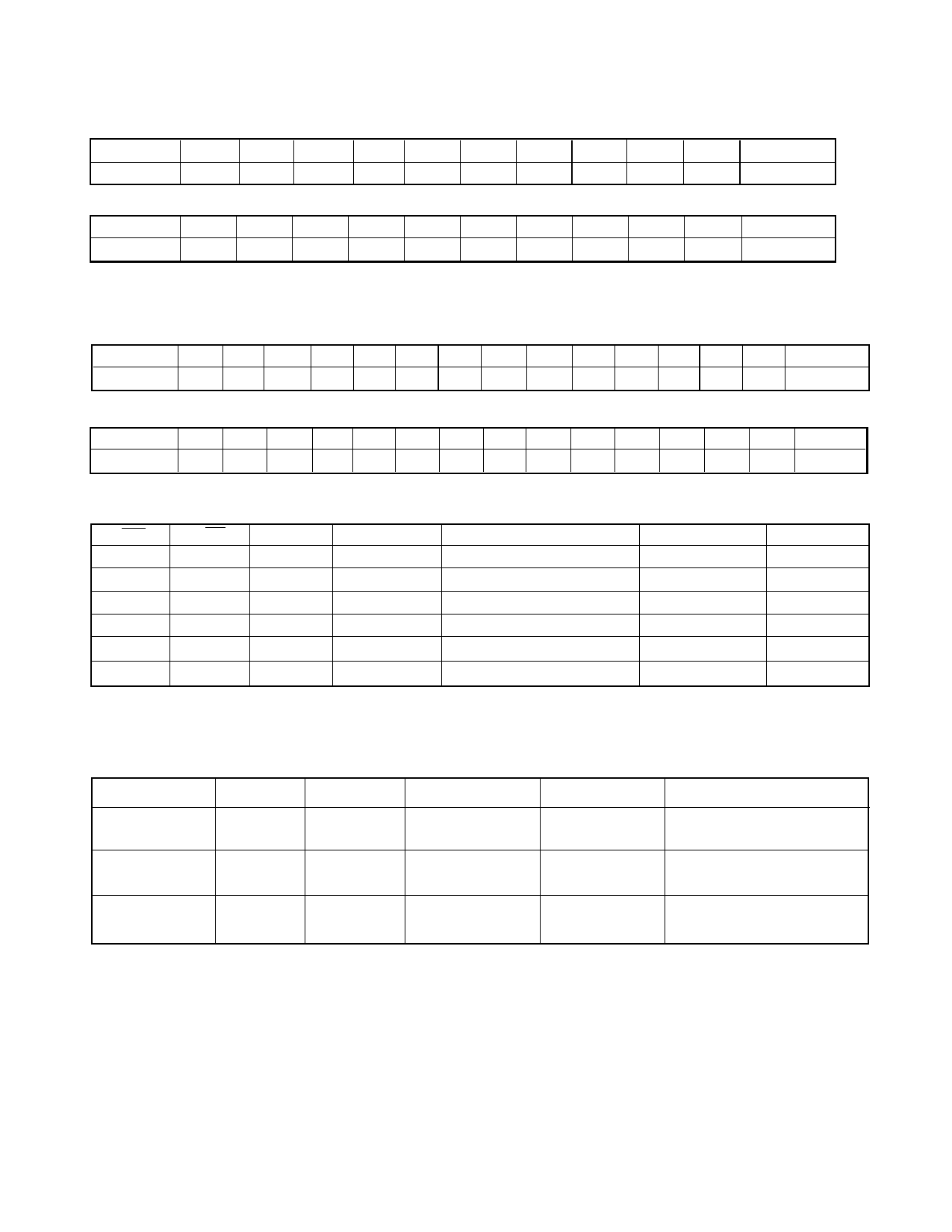
Table 1: Input Data Format and Bit Weighting
Two’s complement signed binary, data range: -1 ≤ SI < 1
SI11
SI10
SI9
SI8
-20
2-1
2-2
2-3
SI7
SI6
SI5
SI4
SI3
SI2
SI1
SI0
2-4
2-5
2-6
2-7
2-8
2-9
2-10
2-11
Unsigned binary, data range: 0 ≤ SI < 256
SI11
SI10
SI9
SI8
27
26
25
24
SI7
SI6
SI5
SI4
SI3
SI2
SI1
SI0
23
22
21
20
2-1
2-2
2-3
2-4
Table 2: Output Data Format and Bit Weighting
Two’s complement signed binary, data range: -1 ≤ SO < 1
SO15
-20
SO14 SO13 SO12 SO11 SO10 SO9 SO8 SO7
2-1 2-2
2-3 2-4
2-5 2-6 2-7 2-8
SO6
2-9
SO5
2-10
SO4
2-11
SO3 SO2
2-12 2-13
SO1
2-14
SO0
2-15
Unsigned binary, data range: 0 ≤ SO < 256
SO15 SO14 SO13 SO12 SO11 SO10 SO9 SO8 SO7
27
26 25
24 23
22
21
20 2-1
SO6
2-2
SO5 SO4
2-3 2-4
SO3 SO2 SO1 SO0
2-5 2-6 2-7 2-8
Table 3: Operation Mode Control
DEC
INT
Sync
0
0
0
0
0
1
0
1
Sync
1
0
Sync
1
0
Sync
1
1
Sync
Mode
Bandpass1
Bandpass2
Decimating
Interpolating
Interpolating
Pass through
Description
21 Tap Bandpass
9 Tap Bandpass Gain=2
Gain=1
Gain=0.5
Gain=1 for unsigned input3
Top 12 bit pass through
Device Latency
18 Clock Cycles
18 Clock Cycles
33 Clock Cycles
33 Clock Cycles
33 Clock Cycles
33 Clock Cycles
Notes
2
2
1
1
2
2
Notes:
1. This operating mode is compatible with TMC2242.
2. This is an enhanced operating mode of the GF9102A.
3. This mode is invoked using the SO0 pin. See I/O Format control below.
Table 4: I/O Format Control
RND2..0
RND = 000
SO03
Output
TCO
0
Input5
Signed
Output5
I_Unsigned
Notes
1
1
Signed
Signed
RND ≠ 000
0
0
Signed
I_Unsigned
1
1
Signed
Signed
RND ≠ 000
1
0
Unsigned4
Unsigned
2
1
Unsigned
Signed
Limit output up to 15 bits
Notes:
1. This operating mode is compatible with TMC2242.
2. This is an enhanced operating mode of the GF9102A.
3. SO0, the LSB of the output is a bi-directional pad with a large pull-down resistor. This pin does not have to be connected.
When this pin is not connected the GF9102A defaults to a mode compatible with the TMC2242.
4. Application notes for the TMC2242 suggest grounding the MSB of the input if the input data is unsigned as
in most A/D converters. This method limits the input to 11 bits and leads to potential output non-saturated type overflow
since the MSB of the output is ignored.
5. Signed: two’s complement binary data.
I_unsigned: invert all bits in signed data except for the MSB; also called inverted offset binary.
Unsigned: invert MSB of signed data; also called offset binary.
5
521 - 26 - 02
Share Link: 