HCC4017BC1 Просмотр технического описания (PDF) - STMicroelectronics
Номер в каталоге
Компоненты Описание
Список матч
HCC4017BC1 Datasheet PDF : 12 Pages
| |||
HCC/HCF4017B/4022B
cycle every 10 clock input cycles in the
HCC/HCF4017B or every 8 clock input cycles in the
HCC/HCF4022B and is used to ripple-clock the suc-
ceeding device in a multi-device counting chain.
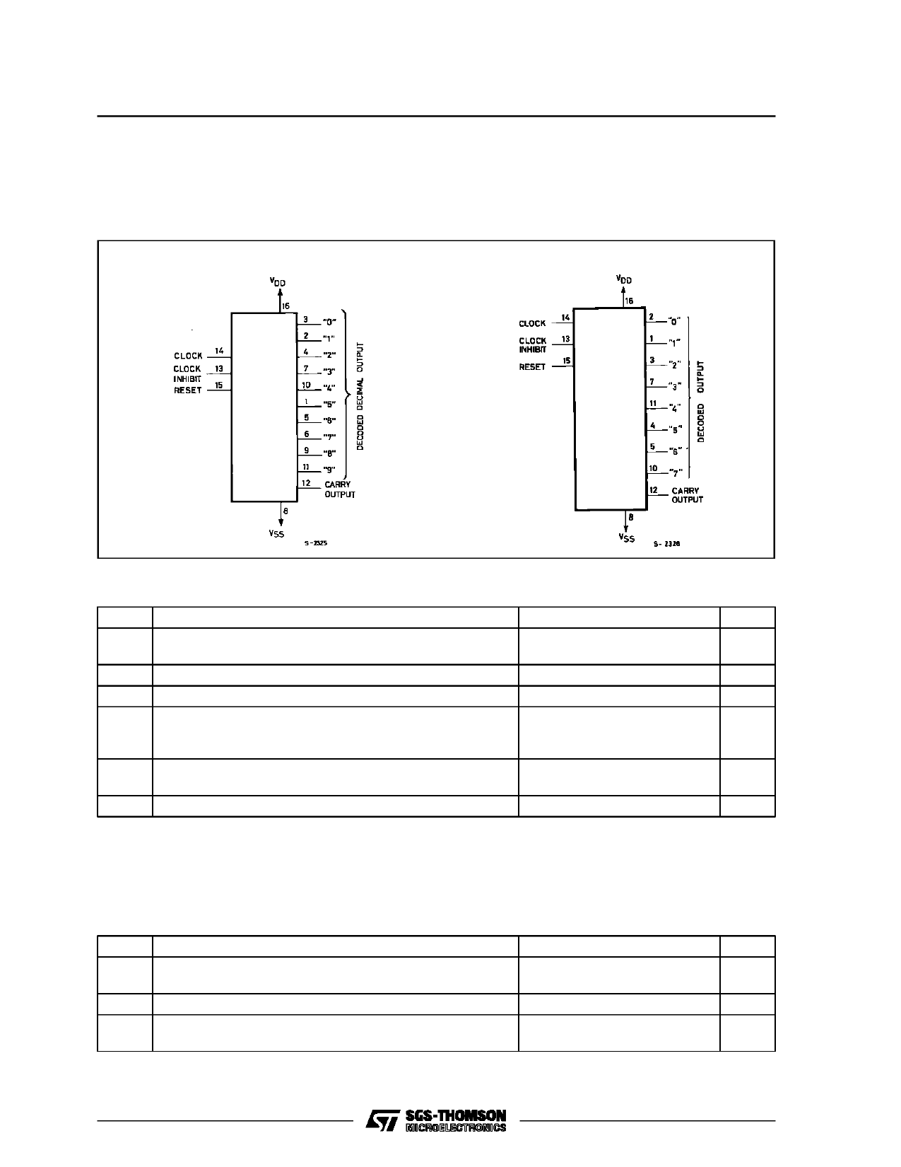
FUNCTIONAL DIAGRAM
4017B
4022B
ABSOLUTE MAXIMUM RATINGS
Symbol
Parameter
Value
Unit
V DD* Supply Voltage : HCC Types
HC F Types
– 0.5 to + 20
V
– 0.5 to + 18
V
VI Input Voltage
II
DC Input Current (any one input)
– 0.5 to VDD + 0.5
V
± 10
mA
Pt o t Total Power Dissipation (per package)
Dissipation per Output Transistor
for To p = Full Package-temperature Range
T o p Operating Temperature : HCC Types
H CF Types
200
mW
100
mW
– 55 to + 125
°C
– 40 to + 85
°C
Ts tg Storage Temperature
– 65 to + 150
°C
Stresses above those listed under ”Absolute Maximum Ratings” may cause permanent damage to the device. This is a stress
rating only and functional operation of the device at these or any other conditions above those indicated in the operational sec-
tions of this specification is not implied. Exposure to absolute maximum rating conditions for external periods may affect device
r eli abil ity .
* All voltages values are referred to VSS pin voltage.
RECOMMENDED OPERATING CONDITIONS
Symbol
Parameter
VDD Supply Voltage : HCC Types
HC F Types
VI Input Voltage
T o p Operating Temperature : HCC Types
H CF Types
Value
3 to 18
3 to 15
0 to VDD
– 55 to + 125
– 40 to + 85
Unit
V
V
V
°C
°C
2/12
Share Link: 