UPC8158 Просмотр технического описания (PDF) - NEC => Renesas Technology
Номер в каталоге
Компоненты Описание
Список матч
UPC8158
NEC => Renesas Technology

UPC8158 Datasheet PDF : 12 Pages
| |||
µPC8158K
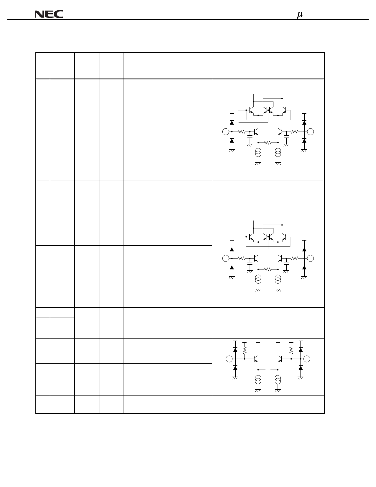
PIN EXPLANATIONS
Supply Pin
Pin
Symbol Voltage Voltage
No.
Note
(V)
(V)
Function and Application
1
Iin
VCC/2
2
Iinb
VCC/2
–
Input for I signal. This input
impedance is 200 kΩ. In the case of
that I/Q input signals are single
ended, amplitude of the signal is
500 m VP-P max.
–
Input for I signal. This input
impedance is 200 kΩ. In the case of
that I/Q input signals are single
ended, VCC/2 biased DC signal
should be input. In the case of the
I/Q input signals are differential,
amplitude of the signal is 500 m VP-P
max.
3 N.C.
–
–
This pin is not connected to internal
circuit. This pin should be opened
or grounded.
4 Qinb
VCC/2
5
Qin
VCC/2
–
Input for Q signal. This input
impedance is 200 kΩ. In the case of
that I/Q input signals are single
ended, amplitude of the signal is
500 m VP-P max.
–
Input for I signal. This input
impedance is 200 kΩ. In the case of
that I/Q input signals are single
ended, VCC/2 biased DC signal
should be input. In case of the I/Q
input signals are differential,
amplitude of the signal is 500 m VP-P
max.
6 N.C.
–
7 N.C.
8 N.C.
–
These pins are not connected to
internal circuit. These pins should
be opened or grounded.
9 LO1inb
–
2.98 Bypass pin of modulator’s local
input. This pin should be decoupled
with 330 pF capacitor.
10 LO1in
–
2.98
11
VCC 2.7 to 4.0
–
Local signal input for modulator.
This pin must be coupled with DC
cut capacitor 330 pF and should be
terminated with 51 Ω resistor.
Supply voltage pin for modulator,
up-converter and AGC circuits.
Internal Equivalent Circuit
1
2
–––––––––––––––––
4
5
–––––––––––––––––
9
10
–––––––––––––––––
Note Pin Voltages are measured on VCC = 3.0 V.
6
Preliminary Data Sheet P13831EJ1V1DS00
Share Link: