UPC8002GR Просмотр технического описания (PDF) - NEC => Renesas Technology
Номер в каталоге
Компоненты Описание
Список матч
UPC8002GR Datasheet PDF : 32 Pages
| |||
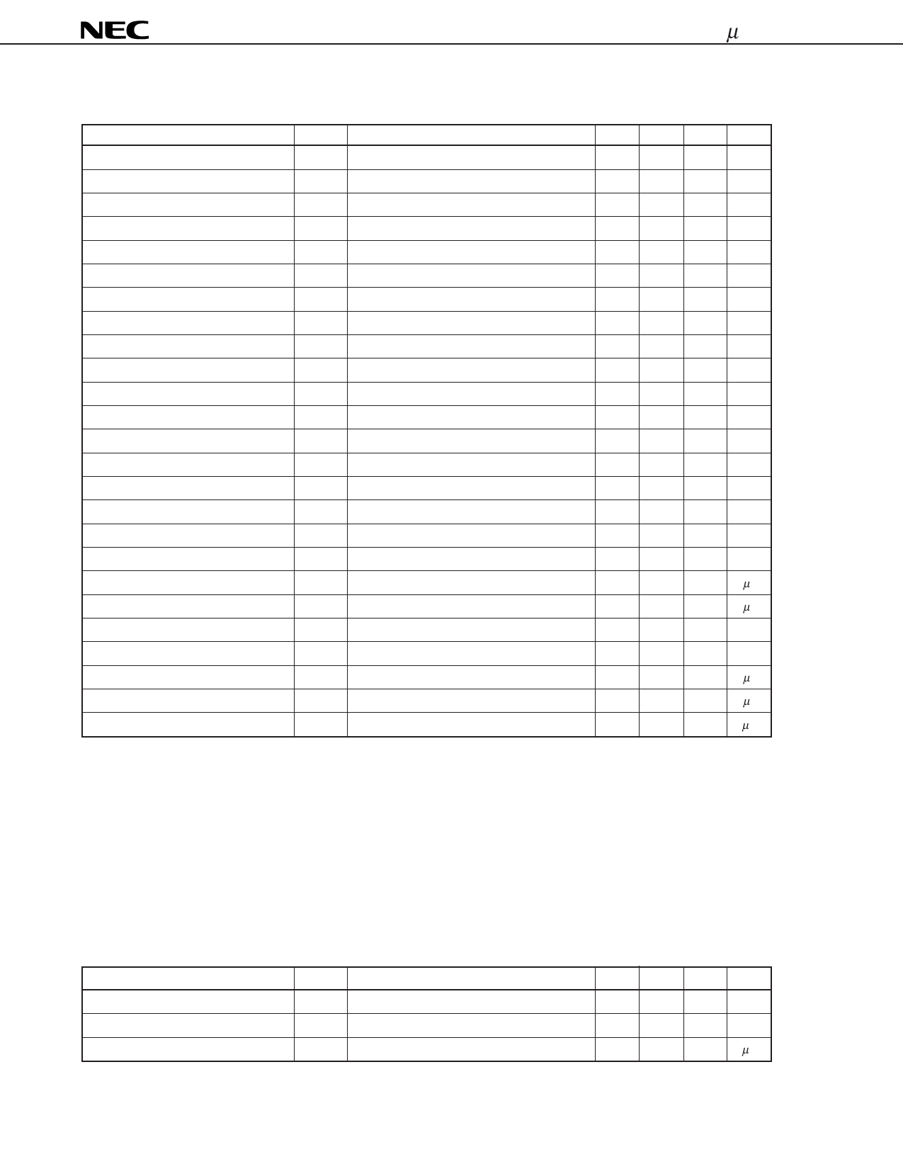
µPC8002
(2) IF Amplifier Section (fIF = 10.7 MHz) 0 dBm = 223.6 mVrms (at 50 Ω)
Parameter
Symbol
Test Condition
Power supply current
ICCI
No signal
Limiting sensitivity
SL
–3 dB point
IF amplifier phase fluctuation
SP
VIF = –70 to –14 dBm
IF amplifier output amplitude
VO
IF2 OUT, VIF = –14 dBm
IF amplifier output amplitude rise time tR
IF2 OUT, VIF = –14 dBm
IF amplifier output amplitude fall time tF
IF2 OUT, VIF = –14 dBm
IF amplifier input resistance
Rin IF1 IN, IF2 IN
IF amplifier input capacitance
Cin IF1 IN, IF2 IN
IF amplifier output resistance
RO IF1 OUT
RSSI linearity
LR
VIF = –94 to –14 dBm
RSSI slope
SR
RSSI intercept
IR
RSSI output voltage 1
VR1
VIF = –14 dBm
RSSI output voltage 2
VR2
VIF = –54 dBm
RSSI output voltage 3
VR3
VIF = –94 dBm
RSSI output voltage 4
VR4 No signal
RSSI output temperature stability
ST
VIF = –94 to –14 dBm
RSSI output dynamic range
DR Note 3
RSSI rise time
trf1
VIF = –14 dBm
RSSI fall time
trf2
VIF = –14 dBm
RSSI output ripple
RR
VIF = –14 dBm
RSSI output resistance
ROR
Power-on rise time
tONI
VPO = 3 V, no signalNote 5
Power-off fall time
tOFI
VPO = 0 VNote 6
Power-off power supply current
ILI
VPO = 0 V
Note 1
Note 2
Note 4
Note 4
MIN. TYP. MAX. Unit
1.7 2.3 mA
–100 –97 dBm
10
deg
0.2
0.3
0.4
Vp-p
8
20
ns
15
25
ns
230 330 430 Ω
3.5 6.0 pF
230 330 430
Ω
±2
dB
18
20
22 mV/dB
–164.7 –148 –134.4 dBm
2.58 2.68 2.78 V
1.76 1.88 2.0
V
0.88 1.08 1.28 V
0.96 1.23 V
±2
dB
80
90
dB
1.0
4
µs
1.6
4
µs
20 mVp-p
25.6 32 38.4 kΩ
5
10
µs
1
3
µs
6
10
µA
Notes 1. Network analyzer RBW = 3 Hz
2. TA = –30 °C to +85 °C
3. Input level range for which drift from the regression expression with VIF = –94 to –14 dBm is ≤ 2 dB
4. Time until the RSSI output reaches the final value ±10 %
5. Time until the RSSI output is within ±10 % of the power-on value
Power-on input voltage (VPO) rise time: 10 ns
6. Time until the power supply current reaches 10 % of the power-on value
Power-on input voltage (VPO) fall time: 10 ns
(3) Power-On/Off Section
Parameter
Power-on input voltage
Power-off input voltage
Power-on input current
Symbol
Test Condition
VON Power-on at VON or above, VCC or below
VOF Power-off at VOF or below, GND or above
ION
VPO = 3 V
MIN. TYP. MAX. Unit
1.5 2.4
V
0.6 1.2
V
40
60
µA
12
Share Link: 