UPC1678G-E2 Просмотр технического описания (PDF) - NEC => Renesas Technology
Номер в каталоге
Компоненты Описание
Список матч
UPC1678G-E2 Datasheet PDF : 16 Pages
| |||
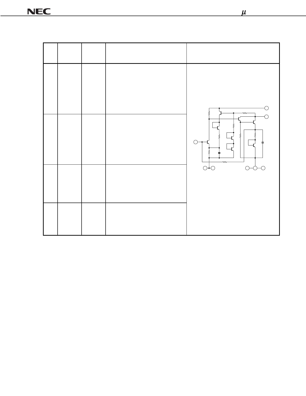
µPC1678G
PIN EXPLANATION
Applied
Pin
Pin Name Voltage
No.
(V)
Function and Applications
Internal Equivalent Circuit
1
INPUT
2
GND
3
4
6
7
–
Signal input pin. A internal matching
circuit, configured with resisters, enables
50 Ω connection over a wide band.
A multi-negative feedback circuit is
designed to cancel the deviations of hFE
and resistance.
This pin must be coupled to signal source
with capacitor for DC cut.
0
Ground pin. This pin should be
connected to system ground with
minimum inductance. Ground pattern on
the board should be formed as widely as
possible. All the ground pins must be
IN 1
connected together with wide ground
pattern to decrease impedance
difference.
8 VCC
5 OUT
5 OUTPUT Voltage
Signal output pin. The inductor must be
as same attached between VCC and output pins to
as VCC
supply current to the internal output
through
transistors.
external
inductor
67
GND
234
GND
2, 3, 4, 6 and 7 are shorted by a lead frame.
8
VCC
4.5 to 5.5 Power supply pin, which biases the
internal input transistors.
This pin should be externally equipped
with bypass capacitor to minimize its
impedance.
Data Sheet P11491EJ4V0DS00
3
Share Link: 