RB5C396 Просмотр технического описания (PDF) - RICOH Co.,Ltd.
Номер в каталоге
Компоненты Описание
Список матч
RB5C396 Datasheet PDF : 93 Pages
| |||
RF5C296/RF5C396L/RB5C396/RF5C396
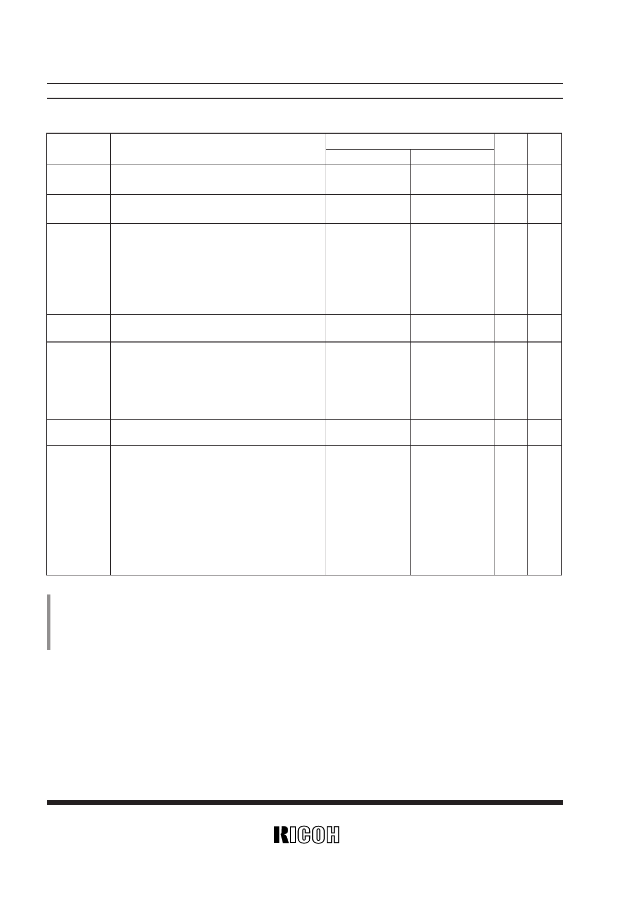
Symbol
Function
CD1#, CD2# Card Detect Input 1 & 2*3
RDY/BSY#
(IREQ#)
REG#
READY/BUSY# input on the memory PC card,
and IREQ# input on the I/O card.
When this signal is “L” memory access is limited
to Attribute memory. During normal access for
I/O, this signal must be kept “L”. During DMA
cycle, this signal must be kept “H”.
This pin may also be used as card side DACK in
DMA mode.
WAIT# Bus Cycle Wait Input from PC Card
WP
(IOIS16#)
Write Protect switch input on the memory PC
card and, IOIS16# is asserted by PC card when
the I/O cycle is 16bit on the I/O.
This pin may also be used as card side DREQ in
DMA mode.
RESET Card Reset Output
INPACK#
Input Acknowledge. “L” is output to INPACK# on
the PCMCIA bus only when I/O ports accessed
during I/O signal read are enabled on PC cards
that support this signal.
When INPACK# signal is enabled for
RF5C296/RF5C396, I/O signal read data will be
output to the system only when the INPACK#
signal is enabled. This pin may also be used as
card side DREQ in DMA mode.
Pin No.
RF5C296
RF5C396*2
10,70
Slot#0 : 10,69
Slot#1 : 73,132
Slot#0 : 39
39
Slot#1 : 101
I/O*1 Drive
I
—
I
—
8
Slot#0 : 8
O(TS) 4mA
Slot#1 : 71
55
Slot#0 : 54
I
—
Slot#1 : 116
69
Slot#0 : 68
Slot#1 : 131
I
—
51
Slot#0 : 51
O(TS) 4mA
Slot#1 : 114
16
Slot#0 : 56
Slot#1 : 119
I
—
*1) I : Input, O : Output, I/O : Input/Output, O (TS) : Tri-State Output.
*2) All card slot interface signal names are pretended with A-(slot#0) and B-(slot#1).
For example, ACA25 to ACA0 are the card address buses to the slot #0.
Pin No. of the RB5C396 differ from those of others. Refer to "PIN CONFIGURATION".
*3) CD1# and CD2# are powered by VCC_AT instead of VCC_SLOT because hot plug-in/out is supported during card slot power is off.
14
Share Link: 