RF5C396 Просмотр технического описания (PDF) - RICOH Co.,Ltd.
Номер в каталоге
Компоненты Описание
Список матч
RF5C396 Datasheet PDF : 93 Pages
| |||
RF5C296/RF5C396L/RB5C396/RF5C396
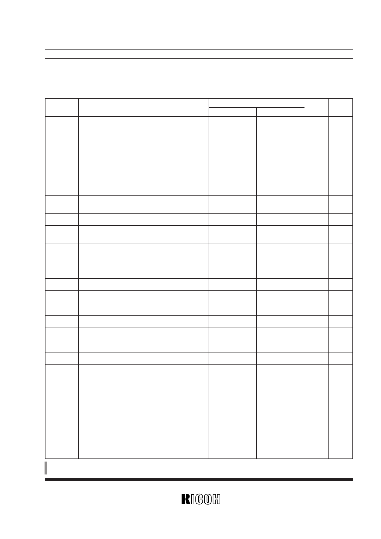
PIN DESCRIPTION
1. ISA Bus Interface
Symbol
Function
LA23 to LA17 ISA Bus System Address 23 to 17
Pin No.
RF5C296
RF5C396*1
96,94,92,89,87,85, 157,155,153,151,
84
149,147,146
SA16 to SA0 ISA Bus System Address 16 to 0
AEN
BALE
Address Enable. High signal is input in DMA
mode.
Address Latch Enable. This signal latches LA23
pin to LA17 pin.
123,122,121,120,
118,117,115,114,
112,110,108,107,
106,104,103,101,
100
126
105
184,183,182,181,
179,178,176,175,
173,171,169,168,
167,165,164,162,
161
187
166
SBHE# System Bus High Byte Enable
98
159
This active low signal indicates that an ISA-bus
REFRESH# refresh cycle is either requested or in progress.
119
180
SD15 to SD0 System Data Bus
71,73,74,75,77,79, 134,135,136,137,
80,81,140,139, 139,141,142,143,
137,136,134,132, 200,199,197,196,
130,129
194,193,190,189
IOR# I/O Port Read
124
185
IOW# I/O Port Write
125
186
MEMR# Memory Read
83
145
MEMW# Memory Write
82
144
IOCS16# 16bit I/O Transfer Mode Chip Select
97
158
MEMCS16# 16bit Memory Transfer Mode Chip Select
99
160
ZEROWS# Zero Wait State
131
191
I/O Channel Ready. This active High signal indi-
IOCHRDY cates that the accessed device on the ISA-bus is
127
188
ready to terminate the bus cycle.
IRQn
Interrupt Request Signal.
IRQ3, IRQ4, IRQ5, IRQ7, IRQ9, IRQ10, IRQ11,
IRQ12, IRQ14, IRQ15. Level mode interrupt or
Edge mode interrupt is programmable. IRQ12
can be used as a LED driver. IRQ9, IRQ10,
IRQ11, or IRQ15 may be used as system side
DACK#, system side DREQ, and system side TC
respectively in DMA mode.
109,111,113,116,
138,95,93,90,86,
88
170,172,174,177,
198,156,154,152,
148,150
* ) I : Input, O : Output, I/O : Input/Output, O (OD) : Open Drain Output, O (TS) : Tri-State Output.
*1) Pin No. of the RB5C396 differ from those of others. Refer to “PIN CONFIGURATION”.
I/O*
I
I
I
I
I
I
I/O
I
I
I
I
O(OD)
O(OD)
O(TS)
O(TS)
O(TS)
Drive
—
—
—
—
—
—
12mA
—
—
—
—
16mA
16mA
12mA
16mA
8mA
11
Share Link: 