TSM1012 Просмотр технического описания (PDF) - STMicroelectronics
Номер в каталоге
Компоненты Описание
Список матч
TSM1012
STMicroelectronics

TSM1012 Datasheet PDF : 8 Pages
| |||
TSM1012
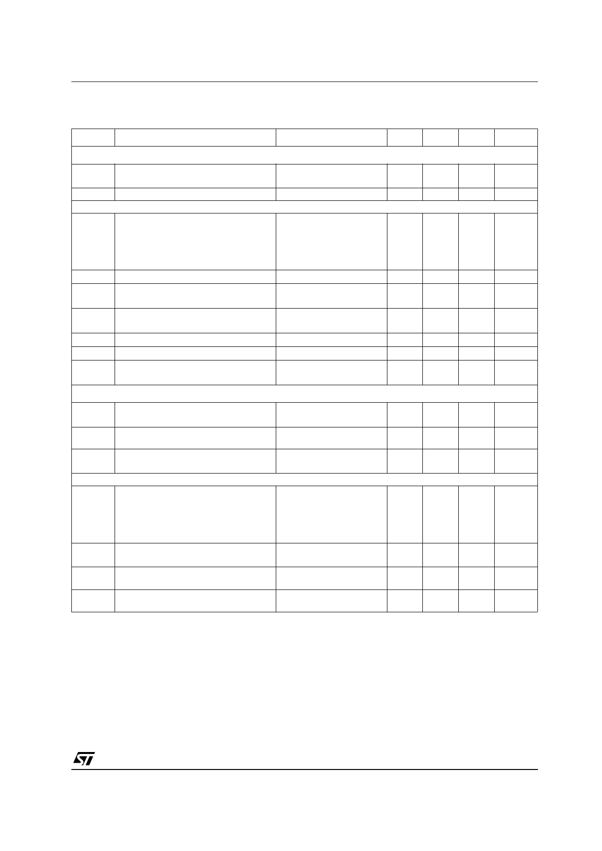
ELECTRICAL CHARACTERISTICS
Tamb = 25°C and Vcc = +18V (unless otherwise specified)
Symbol
Parameter
Test Condition
Min Typ Max Unit
Total Current Consumption
Icc Total Supply Current, excluding current
in Voltage Reference1).
Vz Vcc clamp voltage
Operators
Vio Input Offset Voltage
TSM1012
TSM1012A
DVio
Iio
Input Offset Voltage Drift
Input Offset Current
Iib Input Bias Current
SVR
Vicm
CMR
Supply Voltage Rejection Ration
Input Common Mode Voltage Range
Common Mode Rejection Ratio
Vcc = 18V, no load
Tmin. < Tamb < Tmax.
Icc = 50mA
Tamb = 25°C
Tmin. ≤ Tamb ≤ Tmax.
Tamb = 25°C
Tmin. ≤ Tamb ≤ Tmax.
Tamb = 25°C
Tmin. ≤ Tamb ≤ Tmax.
Tamb = 25°C
Tmin. ≤ Tamb ≤ Tmax.
VCC = 4.5V to 28V
Tamb = 25°C
Tmin. ≤ Tamb ≤ Tmax.
100 180
µA
28
V
1
4
mV
5
0.5
2
3
7
µV/°C
2
30
nA
50
20
150
nA
50
200
65
100
dB
0
Vcc-1.5 V
70
85
dB
60
Output stage
Gm Transconduction Gain. Sink Current
Only2)
Vol Low output voltage at 5 mA sinking
current
Tamb = 25°C
Tmin. ≤ Tamb ≤ Tmax.
Tmin. ≤ Tamb ≤ Tmax.
1
0.5
1
mA/mV
250 400
mV
Ios Output Short Circuit Current. Output to Tamb = 25°C
6
10
mA
(Vcc-0.6V). Sink Current Only
Tmin. ≤ Tamb ≤ Tmax.
5
Voltage reference
Vref
∆Vref
Reference Input Voltage
TSM1012 1% precision
TSM1012A 0.5% precision
Reference Input Voltage Deviation Over
Temperature Range
Tamb = 25°C
Tmin. ≤ Tamb ≤ Tmax.
Tamb = 25°C
Tmin. ≤ Tamb ≤ Tmax.
Tmin. ≤ Tamb ≤ Tmax.
1.238 1.25 1.262
1.225
1.273
V
1.244 1.25 1.256
1.237
1.261
20
30
mV
RegLine Reference input voltage deviation over Iload = 1mA
Vcc range.
20
mV
RegLoad Reference input voltage deviation over Vcc = 18V,
output current.
0 < Iload < 2.5mA
10
mV
1. Test conditions: pin 2 and 6 connected to GND, pin 4 and 5 connected to 1.25V, pin 3 connected to 200mV.
2. The current depends on the difference voltage between the negative and the positive inputs of the amplifier. If the voltage on the minus
input is 1mV higher than the positive amplifier, the sinking current at the output OUT will be increased by Gm*1mA.
3/8
Share Link: