TRC104 Просмотр технического описания (PDF) - RF Monolithics, Inc
Номер в каталоге
Компоненты Описание
Список матч
TRC104 Datasheet PDF : 33 Pages
| |||
3.3 PLL
The PLL channel is set with the Ch_Num bits in configuration register 0x00. In transmit mode, the PLL is normally
turned on with the falling edge of the MODE input. The TRC104 transmits the data after the PLL locks and the
power amplifier has ramped up to its programmed level. PLL lock time is typically 170 µs. It is possible to enable
and lock the PLL before the falling edge of MODE input. This can provides a shorter transition time to transmit.
The PLL pre-start delay time is adjustable from 20 µs up to 5 ms. The value of PLL_ON in register 0x14 sets this
time. The pre-start delay timer is triggered on the rising edge of MODE as shown in Figure 5. The value of
PLL_ON determines the delay time from the rising edge of MODE before the PLL is enabled. Care must be taken
to carefully calculate the write time of the data packet into the transmit FIFO so that the TRC104 does not enable
the transmitter and begin sending data before the data packet is fully written to the FIFO, in which case the
TRC104 will discard the current packet.
P L L P r e -s ta r t T im in g
M ODE
P L L S ta te
PLL O FF
P L L L O C K IN G
PLL O N
PLL O FF
D a ta
D ELA Y
D E L A Y : P r e - s ta r t d e la y in te r v a l
R F D a ta T r a n s m is s io n
Figure 5
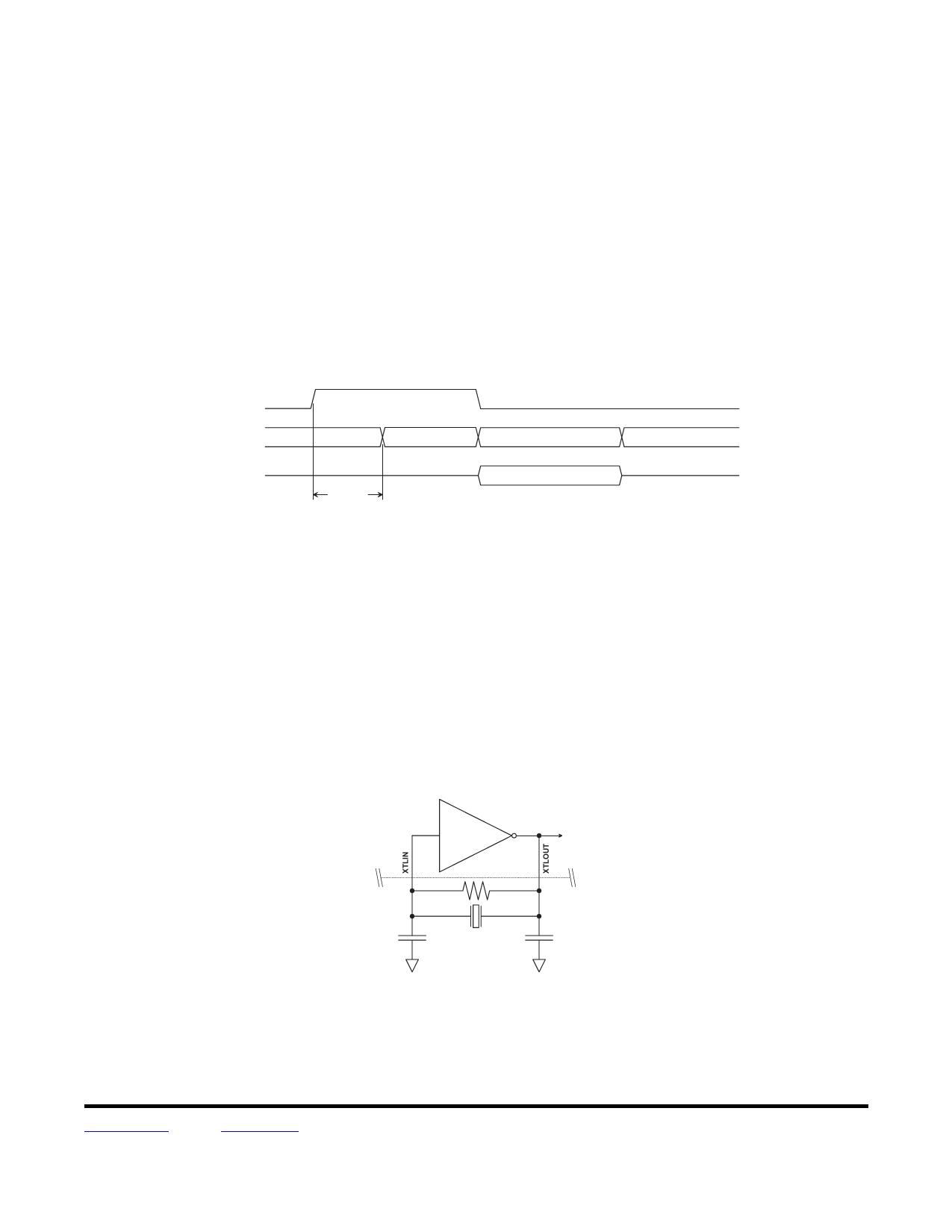
3.4 Crystal Oscillator
At the 1 Mb/s RF data rate, the TRC104 uses a 16 MHz crystal. At the 250 kb/s RF data rate, the TRC104 can
use any one of five standard crystal frequencies: 4, 8, 12, 16, or 20 MHz. The crystal frequency is configured by
setting the FXTAL bits in register 0x01. At the 250 kb/s data rate, the TRC104’s power consumption is reduced by
using one of the lower crystal frequencies. The total load capacitance CL seen between the XTLIN and XTLOUT
terminals is composed primarily of CIN and COUT in series, as shown if Figure 6:
CL = 1/((1/CIN) + (1/COUT) ) + CSTRAY, where CSTRAY is the capacitance associated with the PCB layout
T R C 1 0 4 C r y s ta l O s c illa to r Im p le m e n ta tio n
9
8
C IN
C OUT
Figure 6
A typical value for CSTRAY is 1 pF. The values of CIN and COUT should be approximately equal and chosen so that
CL matches the load capacitance specified for the crystal. A typical CL value for a 16 MHz crystal is 12 pF. The
www.RFM.com E-mail: info@rfm.com
©2009 by RF Monolithics, Inc.
Technical support +1.800.704.6079
Page 10 of 33
TRC104 - 08/13/09
Share Link: 