IDT723622(2015) Просмотр технического описания (PDF) - Integrated Device Technology
Номер в каталоге
Компоненты Описание
Список матч
IDT723622
(Rev.:2015)
(Rev.:2015)
Integrated Device Technology

IDT723622 Datasheet PDF : 24 Pages
| |||
IDT723622/723632/723642 CMOS SyncBiFIFO™
256 x 36 x 2, 512 x 36 x 2, 1,024 x 36 x 2
COMMERCIAL TEMPERATURE RANGE
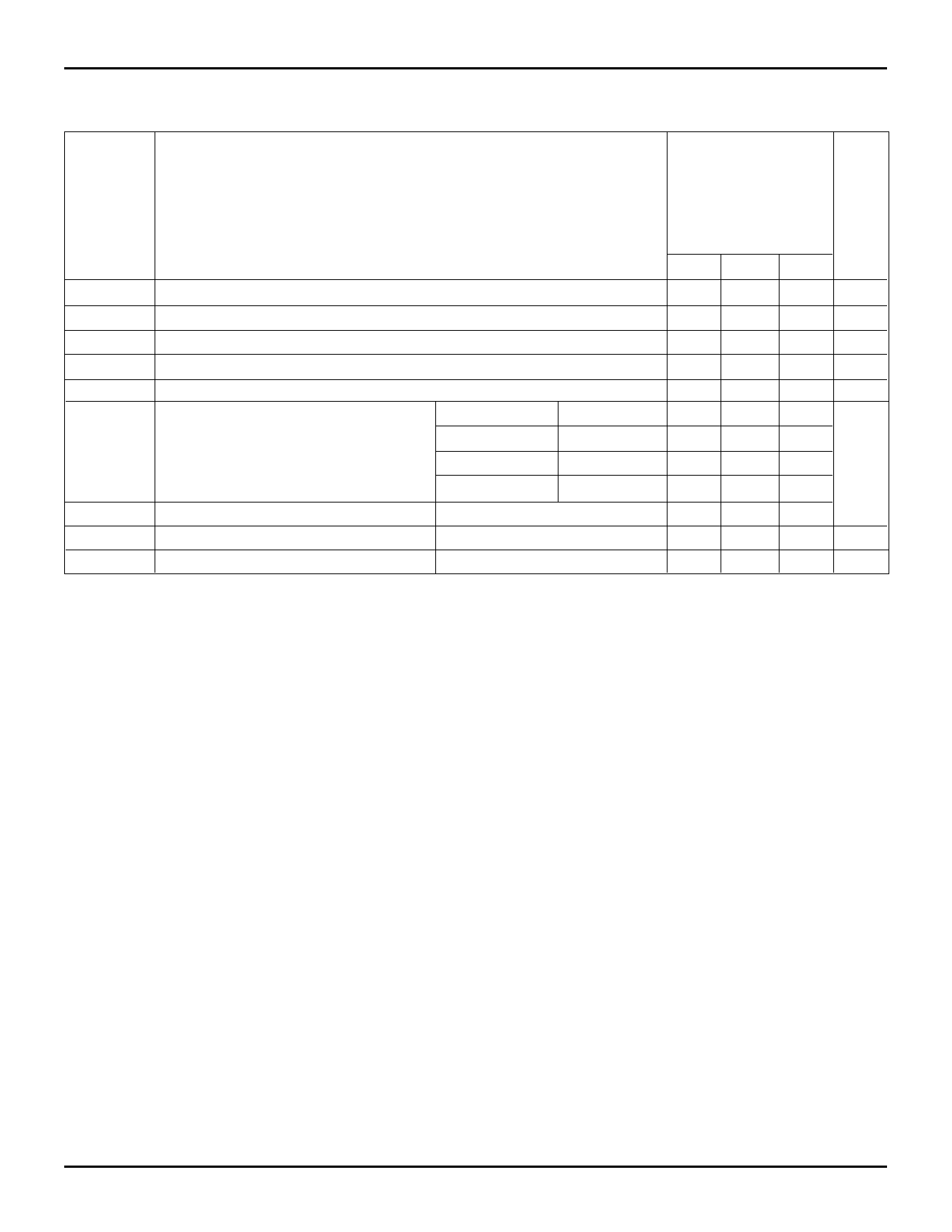
TIMING REQUIREMENTS OVER RECOMMENDED RANGES OF SUPPLY
VOLTAGE AND OPERATING FREE-AIR TEMPERATURE
(Commercial: VCC = 5V ± 10%, TA = 0°C to +70°C)
Symbol
Parameter
Commercial
IDT723622L15
IDT723632L15
IDT723642L15
Min.
Max.
Unit
fS
Clock Frequency, CLKA or CLKB
—
66.7
MHz
tCLK Clock Cycle Time, CLKA or CLKB
15
—
ns
tCLKH Pulse Duration, CLKA or CLKB HIGH
6
—
ns
tCLKL Pulse Duration, CLKA and CLKB LOW
6
—
ns
tDS
Setup Time, A0-A35 before CLKA↑ and B0-B35 before CLKB↑
4
—
ns
tENS1 Setup Time, CSA and W/RA before CLKA↑; CSB and W/RB before CLKB↑
4.5
—
ns
tENS2 Setup Time, ENA and MBA, before CLKA↑; ENB and MBB before CLKB↑
4.5
—
ns
tRSTS Setup Time, RST1 or RST2 LOW before CLKA or CLKB (2)
5
—
ns
tFSS Setup Time, FS0 and FS1 before RST1 and RST2 HIGH
7.5
—
ns
tDH
Hold Time, A0-A35 after CLKA↑ and B0-B35 after CLKB↑
1
—
ns
tENH Hold Time, CSA, W/RA, ENA, and MBA after CLKA↑; CSB, W/RB, ENB,
and MBB after CLKB↑
1
—
ns
tRSTH Hold Time, RST1 or RST2 LOW after CLKA↑ or CLKB↑(2)
4
—
ns
tFSH Hold Time, FS0 and FS1 after RST1 and RST2 HIGH
2
—
ns
tSKEW1(2) Skew Time, between CLKA↑ and CLKB↑ for ORA, ORB, IRA, and IRB
7.5
—
ns
tSKEW2(2,3) Skew Time, between CLKA↑ and CLKB↑ for AEA, AEB, AFA, and AFB
12
—
ns
NOTES:
1. Requirement to count the clock edge as one of at least four needed to reset a FIFO.
2. Skew time is not a timing constraint for proper device operation and is only included to illustrate the timing relationship between CLKA cycle and CLKB cycle.
3. Designsimulated,nottested.
7
Share Link: