IDT72261L25TFB Просмотр технического описания (PDF) - Integrated Device Technology
Номер в каталоге
Компоненты Описание
Список матч
IDT72261L25TFB Datasheet PDF : 30 Pages
| |||
IDT72261/72271 SyncFIFO™
16,384 x 9, 32,768 x 9
MILITARY AND COMMERCIAL TEMPERATURE RANGES
AC ELECTRICAL CHARACTERISTICS(1)
(Commercial: VCC = 5V ± 10%, TA = 0°C to +70°C; Military: VCC = 5V ± 10%, TA = –55°C to +125°C)
Symbol
fS
tA
tCLK
tCLKH
tCLKL
tDS
tDH
tENS
tENH
tLDS
tLDH
tRS
tRSS
tRSR
tRSF
tFWFT
tRTS
tOLZ
tOE
tOHZ
tWFF
tREF
tPAF
tPAE
tHF
tSKEW1
tSKEW2
Parameter
Clock Cycle Frequency
Data Access Time
Clock Cycle Time
Clock High Time
Clock Low Time
Data Set-up Time
Data Hold Time
Enable Set-up Time
Enable Hold Time
Load Set-up Time
Load Hold Time
Reset Pulse Width(3)
Reset Set-up Time
Reset Recovery Time
Reset to Flag and Output Time
Mode Select Time
Retransmit Set-Up Time
Output Enable to Output in Low Z(4)
Output Enable to Output Valid
Output Enable to Output in High Z(4)
Write Clock to FF or IR
Read Clock to EF or OR
Write Clock to PAF
Read Clock to PAE
Clock to HF
Skew time between RCLK and WCLK
for FF and IR
Skew time between RCLK and
WCLK for PAE and PAF
Commercial
72261L10
72271L10
72261L12
72271L12
Min. Max. Min. Max.
— 100 — 83.3
2
8
2
9
10 — 12 —
4.5 — 5 —
4.5(2) —
5(2)
—
3.5 — 3.5 —
0—0—
3.5 — 3.5 —
0—0—
3.5 — 3.5 —
6.5 — 8.5 —
10 — 12 —
10 — 12 —
10 — 12 —
— 10 — 12
0—0—
3.5 — 3.5 —
0—0—
3
7
3 7.5
3
7
3 7.5
—8—9
—8—9
–
8—9
—8—9
— 16 — 18
8 — 10 —
Com'l & Mil. Commercial
72261L15
72271L15
72261L20
72271L20
Min. Max. Min. Max.
— 66.7 — 50
2
10 2
12
15 — 20 —
6
—8
—
6(2)
—
8
—
4
—5
—
1
—1
—
4
—5
—
1
—1
—
4
—5
—
10 — 10 —
15 — 20 —
15 — 20 —
15 — 20 —
— 15 — 20
0
—0
—
4
—5
—
0
—0
—
3
8
3
10
3
8
3
10
— 10 — 12
— 10 — 12
— 10 — 12
— 10 — 12
— 20 — 22
12 — 15 —
Military
72261L25
72271L25
Min. Max.
— 40
3
15
25 —
10 —
10 —
6
—
1
—
6
—
1
—
6
—
10 —
25 —
25 —
25 —
— 25
0
—
6
—
0
—
3
13
3
13
— 15
— 15
— 15
— 15
— 25
20 —
Unit
MHz
ns
ns
ns
ns
ns
ns
ns
ns
ns
ns
ns
ns
ns
ns
ns
ns
ns
ns
ns
ns
ns
ns
ns
ns
ns
15 — 18 — 21 — 25 — 35 — ns
NOTES:
1. All AC timings apply to both Standard IDT Mode and First Word Fall
Through Mode.
2. For the RCLK line: tCLKL (min.) = 7 ns only when reading the offsets from
the programmable flag registers; otherwise, use the table value. For the
WCLK line, use the tCLKL (min.) value given in the table.
3. Pulse widths less than minimum values are not allowed.
4. Values guaranteed by design, not currently tested.
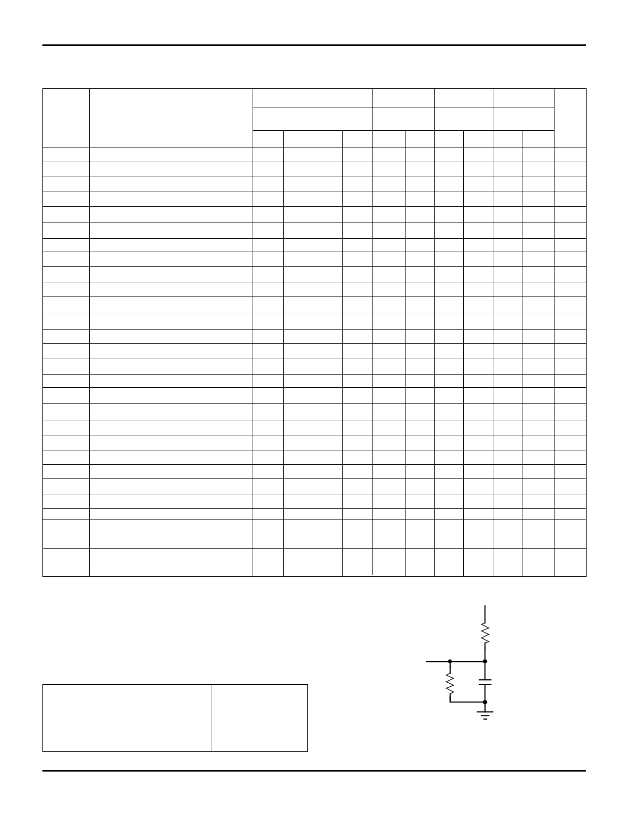
AC TEST CONDITIONS
Input Pulse Levels
Input Rise/Fall Times
Input Timing Reference Levels
Output Reference Levels
Output Load
GND to 3.0V
3ns
1.5V
1.5V
See Figure 1
3097 tbl 08
3097 tbl 06
5V
D.U.T.
680Ω
1.1K
30pF*
3036 drw 04
Figure 1. Output Load
* Includes jig and scope capacitances.
6
Share Link: 