TMC3533 Просмотр технического описания (PDF) - Fairchild Semiconductor
Номер в каталоге
Компоненты Описание
Список матч
TMC3533 Datasheet PDF : 12 Pages
| |||
PRODUCT SPECIFICATION
TMC3533
Application Notes
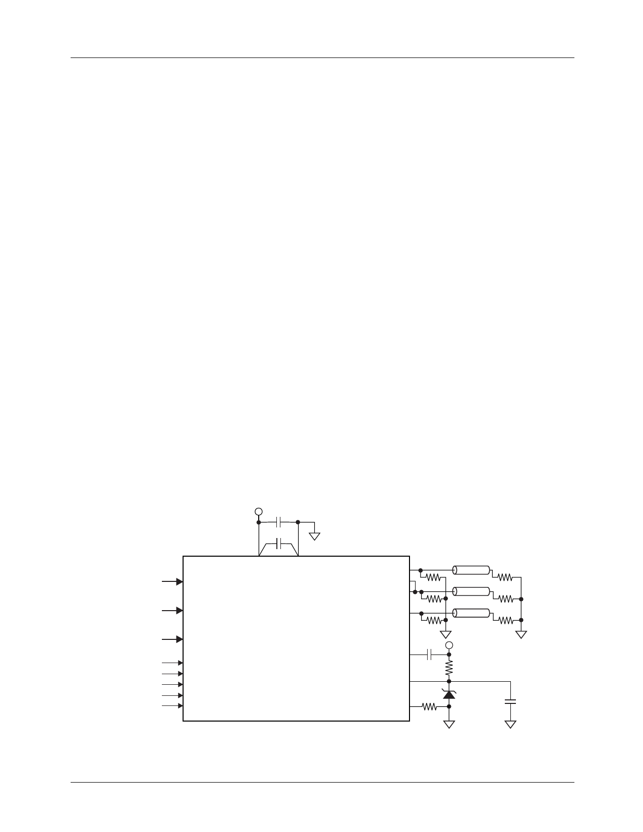
Figure 4 illustrates a typical TMC3533 interface circuit. In
this example, an optional 1.2 Volt bandgap reference is con-
nected to the VREF output, overriding the internal voltage
reference source.
Grounding
It is important that the TMC3533 power supply is well-regu-
lated and free of high-frequency noise. Careful power supply
decoupling will ensure the highest quality video signals at
the output of the circuit. The TMC3533 has separate analog
and digital circuits. To keep digital system noise from the
D/A converter, it is recommended that power supply voltages
(VDD) come from the system analog power source and all
ground connections (GND) be made to the analog ground
plane. Power supply pins should be individually decoupled
at the pin.
Printed Circuit Board Layout
Designing with high-performance mixed-signal circuits
demands printed circuits with ground planes. Overall system
performance is strongly influenced by the board layout.
Capacitive coupling from digital to analog circuits may
result in poor D/A conversion. Consider the following sug-
gestions when doing the layout:
1. Keep the critical analog traces (VREF, IREF, COMP,
IOS, IOR, IOG, IOB) as short as possible and as far as
possible from all digital signals. The TMC3533 should
be located near the board edge, close to the analog out-
put connectors.
2. The power plane for the TMC3533 should be separate
from that which supplies the digital circuitry. A single
power plane should be used for all of the VDD pins. If
the power supply for the TMC3533 is the same as that of
the system's digital circuitry, power to the TMC3533
should be decoupled with 0.1µF and 0.01µF capacitors
and isolated with a ferrite bead.
3. The ground plane should be solid, not cross-hatched.
Connections to the ground plane should have very short
leads.
4. If the digital power supply has a dedicated power plane
layer, it should not be placed under the TMC3533, the
voltage reference, or the analog outputs. Capacitive cou-
pling of digital power supply noise from this layer to the
TMC3533 and its related analog circuitry can have an
adverse effect on performance.
5. CLK should be handled carefully. Jitter and noise on
this clock will degrade performance. Terminate the
clock line carefully to eliminate overshoot and ringing.
Related Products
• TMC3003 Triple 10-bit 80 Msps D/A Converter
• TMC2242C/TMC2243/TMC2246A Video Filters
• TMC2081 Digital Video Mixer
• TMC3503 Triple Video D/A Converter, 5V
• TMC22x5y Video Decoder
RED PIXEL
INPUT
GREEN PIXEL
INPUT
BLUE PIXEL
INPUT
CLOCK
SYNC
BLANK
WHITE
SLEEP
R7-0
G7-0
B7-0
CLK
SYNC
BLANK
WHITE
SLEEP
+3.3V
10µF
0.1µF
VDD
GND
TMC3533
Triple 8-bit
D/A Converter
IO R
IO S
IO G
IO B
COMP
VREF
RREF
75Ω
75Ω
Red
ZO=75Ω
75Ω
Green w/Sync
ZO=75Ω 75Ω
Blue
ZO=75Ω
75Ω
75Ω
+3.3V
0.1µF 3.3kΩ
572Ω
LM185-1.2
(Optional)
0.1µF
Figure 4. Typical Interface Circuit
65-3533-05
REV. 0.9.1 11/24/99
9
Share Link: 