MC14043BD(2000) Просмотр технического описания (PDF) - ON Semiconductor
Номер в каталоге
Компоненты Описание
Список матч
MC14043BD Datasheet PDF : 8 Pages
| |||
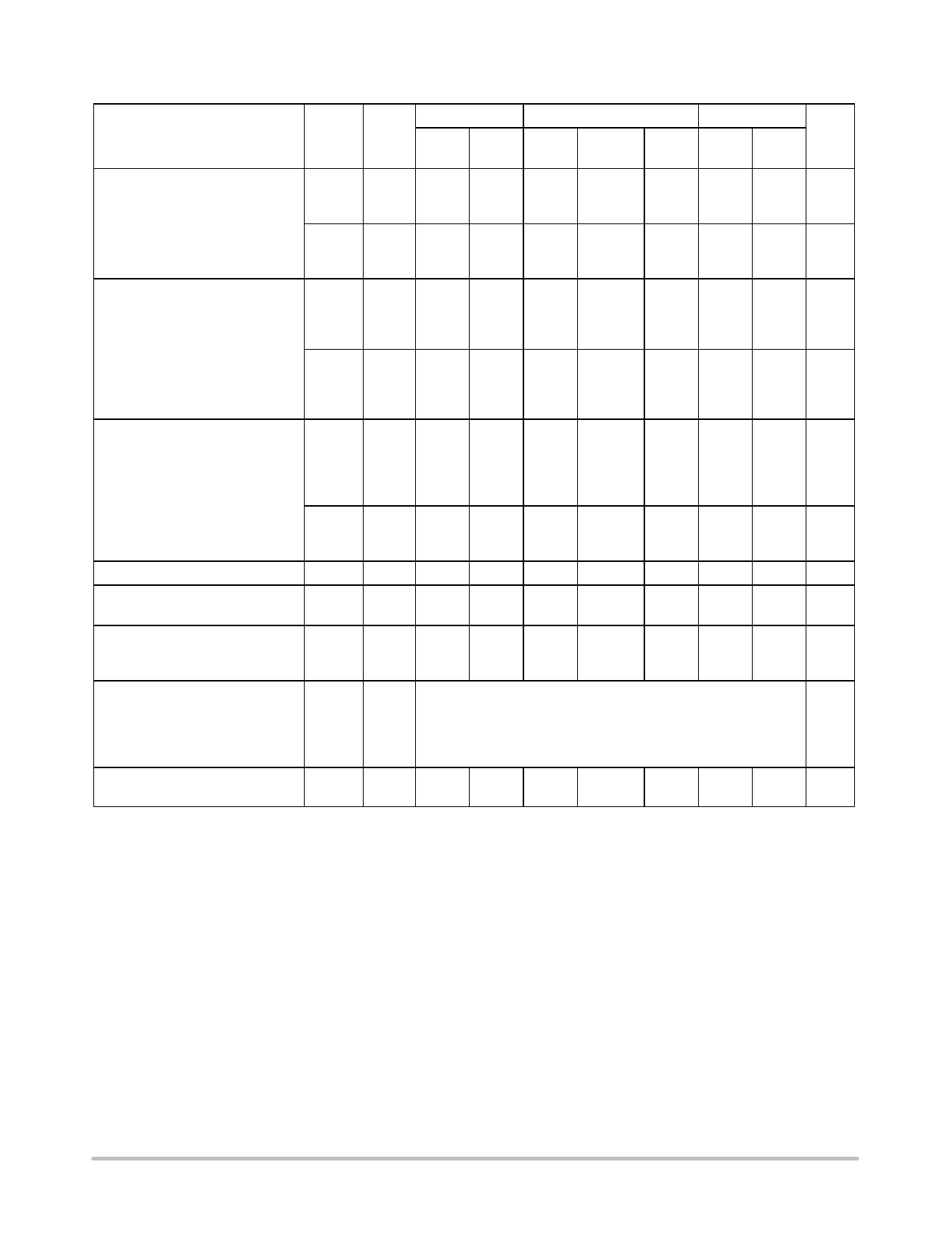
MC14043B, MC14044B
ÎÎÎÎÎÎÎÎÎÎÎÎÎÎÎÎÎÎÎÎÎÎÎÎÎÎÎÎÎÎÎÎÎ ELECTRICAL CHARACTERISTICS (Voltages Referenced to VSS)
ÎÎÎÎÎÎÎÎÎÎÎÎÎÎÎÎÎÎÎÎÎÎÎÎÎÎÎÎÎÎÎÎÎÎÎÎÎÎÎÎÎÎÎÎÎÎÎÎÎÎÎÎÎÎÎÎÎÎÎÎÎÎÎÎÎÎ Characteristic
VDD
– 55_C
25_C
125_C
Symbol Vdc
Min
Max
Min
Typ (4.)
Max
Min
Max
ÎÎÎÎÎÎÎÎÎÎÎÎÎÎÎÎÎÎÎÎÎÎÎÎÎÎÎÎÎÎÎÎÎ Output Voltage
ÎÎÎÎÎÎÎÎÎÎÎÎÎÎÎÎÎÎÎÎÎÎÎÎÎÎÎÎÎÎÎÎÎ Vin = VDD or 0
“0” Level VOL
5.0
10
15
—
0.05
—
—
0.05
—
—
0.05
—
0
0.05
—
0.05
0
0.05
—
0.05
0
0.05
—
0.05
ÎÎÎÎÎÎÎÎÎÎÎÎÎÎÎÎÎÎÎÎÎÎÎÎÎÎÎÎÎÎÎÎÎÎÎÎÎÎÎÎÎÎÎÎÎÎÎÎÎÎÎÎÎÎÎÎÎÎÎÎÎÎÎÎÎÎ Vin = 0 or VDD
“1” Level VOH
5.0
4.95
—
4.95
5.0
10
9.95
—
9.95
10
15
14.95
—
14.95
15
—
4.95
—
—
9.95
—
—
14.95
—
ÎÎÎÎÎÎÎÎÎÎÎÎÎÎÎÎÎÎÎÎÎÎÎÎÎÎÎÎÎÎÎÎÎ Input Voltage
“0” Level VIL
ÎÎÎÎÎÎÎÎÎÎÎÎÎÎÎÎÎÎÎÎÎÎÎÎÎÎÎÎÎÎÎÎÎ (VO = 4.5 or 0.5 Vdc)
5.0
—
1.5
—
ÎÎÎÎÎÎÎÎÎÎÎÎÎÎÎÎÎÎÎÎÎÎÎÎÎÎÎÎÎÎÎÎÎ (VO = 9.0 or 1.0 Vdc)
10
—
3.0
—
(VO = 13.5 or 1.5 Vdc)
15
—
4.0
—
ÎÎÎÎÎÎÎÎÎÎÎÎÎÎÎÎÎÎÎÎÎÎÎÎÎÎÎÎÎÎÎÎÎ “1”Level VIH
ÎÎÎÎÎÎÎÎÎÎÎÎÎÎÎÎÎÎÎÎÎÎÎÎÎÎÎÎÎÎÎÎÎ (VO = 0.5 or 4.5 Vdc)
5.0
3.5
—
3.5
ÎÎÎÎÎÎÎÎÎÎÎÎÎÎÎÎÎÎÎÎÎÎÎÎÎÎÎÎÎÎÎÎÎ (VO = 1.0 or 9.0 Vdc)
10
7.0
—
7.0
(VO = 1.5 or 13.5 Vdc)
15
11
—
11
2.25
4.50
6.75
2.75
5.50
8.25
1.5
—
1.5
3.0
—
3.0
4.0
—
4.0
—
3.5
—
—
7.0
—
—
11
—
ÎÎÎÎÎÎÎÎÎÎÎÎÎÎÎÎÎÎÎÎÎÎÎÎÎÎÎÎÎÎÎÎÎ Output Drive Current
ÎÎÎÎÎÎÎÎÎÎÎÎÎÎÎÎÎÎÎÎÎÎÎÎÎÎÎÎÎÎÎÎÎ (VOH = 2.5 Vdc)
ÎÎÎÎÎÎÎÎÎÎÎÎÎÎÎÎÎÎÎÎÎÎÎÎÎÎÎÎÎÎÎÎÎ (VOH = 4.6 Vdc)
(VOH = 9.5 Vdc)
ÎÎÎÎÎÎÎÎÎÎÎÎÎÎÎÎÎÎÎÎÎÎÎÎÎÎÎÎÎÎÎÎÎ (VOH = 13.5 Vdc)
ÎÎÎÎÎÎÎÎÎÎÎÎÎÎÎÎÎÎÎÎÎÎÎÎÎÎÎÎÎÎÎÎÎ (VOL = 0.4 Vdc)
ÎÎÎÎÎÎÎÎÎÎÎÎÎÎÎÎÎÎÎÎÎÎÎÎÎÎÎÎÎÎÎÎÎ (VOL = 0.5 Vdc)
(VOL = 1.5 Vdc)
ÎÎÎÎÎÎÎÎÎÎÎÎÎÎÎÎÎÎÎÎÎÎÎÎÎÎÎÎÎÎÎÎÎ Input Current
ÎÎÎÎÎÎÎÎÎÎÎÎÎÎÎÎÎÎÎÎÎÎÎÎÎÎÎÎÎÎÎÎÎ Input Capacitance
ÎÎÎÎÎÎÎÎÎÎÎÎÎÎÎÎÎÎÎÎÎÎÎÎÎÎÎÎÎÎÎÎÎ (Vin = 0)
ÎÎÎÎÎÎÎÎÎÎÎÎÎÎÎÎÎÎÎÎÎÎÎÎÎÎÎÎÎÎÎÎÎ Quiescent Current
(Per Package)
IOH
Source
Sink IOL
Iin
Cin
IDD
ÎÎÎÎÎÎÎÎÎÎÎÎÎÎÎÎÎÎÎÎÎÎÎÎÎÎÎÎÎÎÎÎÎÎÎÎÎÎÎÎÎÎÎÎÎÎÎÎÎÎÎÎÎÎÎÎÎÎÎÎÎÎÎÎÎÎ Total Supply Current (5.) (6.)
IT
ÎÎÎÎÎÎÎÎÎÎÎÎÎÎÎÎÎÎÎÎÎÎÎÎÎÎÎÎÎÎÎÎÎ (Dynamic plus Quiescent,
Per Package)
ÎÎÎÎÎÎÎÎÎÎÎÎÎÎÎÎÎÎÎÎÎÎÎÎÎÎÎÎÎÎÎÎÎ (CL = 50 pF on all outputs all
ÎÎÎÎÎÎÎÎÎÎÎÎÎÎÎ ÎÎÎÎÎÎÎÎÎÎÎÎÎÎÎÎÎÎ buffers switching)
5.0 – 3.0
—
– 2.4
– 4.2
5.0 – 0.64 — – 0.51 – 0.88
10
– 1.6
—
– 1.3 – 2.25
15
– 4.2
—
– 3.4
– 8.8
—
– 1.7
—
— – 0.36 —
—
– 0.9
—
—
– 2.4
—
5.0
0.64
—
0.51
0.88
10
1.6
—
1.3
2.25
15
4.2
—
3.4
8.8
—
0.36
—
—
0.9
—
—
2.4
—
15
—
± 0.1
— ± 0.00001 ± 0.1
—
± 1.0
—
—
—
—
5.0
7.5
—
—
5.0
—
1.0
—
0.002
1.0
—
30
10
—
2.0
—
0.004
2.0
—
60
15
—
4.0
—
0.006
4.0
—
120
5.0
IT = (0.58 µA/kHz) f + IDD
10
IT = (1.15 µA/kHz) f + IDD
15
IT = (1.73 µA/kHz) f + IDD
ÎÎÎÎÎÎÎÎÎÎÎÎÎÎÎÎÎÎÎÎÎÎÎÎÎÎÎÎÎÎÎÎÎ Three–State Output Leakage
Current
ITL
15
—
± 0.1
— ± 0.0001 ± 0.1
—
± 3.0
ÎÎÎÎÎÎÎÎÎÎÎÎÎÎÎÎÎÎÎÎÎÎÎÎÎÎÎÎÎÎÎÎÎÎÎÎÎÎÎÎÎÎÎÎÎÎÎÎÎÎÎÎÎÎÎÎÎÎÎÎÎÎÎÎÎÎ 4. Data labelled “Typ” is not to be used for design purposes but is intended as an indication of the IC’s potential performance.
Unit
Vdc
Vdc
Vdc
Vdc
mAdc
mAdc
µAdc
pF
µAdc
µAdc
µAdc
5. The formulas given are for the typical characteristics only at 25_C.
6. To calculate total supply current at loads other than 50 pF:
IT(CL) = IT(50 pF) + (CL – 50) Vfk
where: IT is in µA (per package), CL in pF, V = (VDD – VSS) in volts, f in kHz is input frequency, and k = 0.004.
http://onsemi.com
3
Share Link: 