MBM29F033C Просмотр технического описания (PDF) - Fujitsu
Номер в каталоге
Компоненты Описание
Список матч
MBM29F033C Datasheet PDF : 46 Pages
| |||
MBM29F033C-70/-90/-12
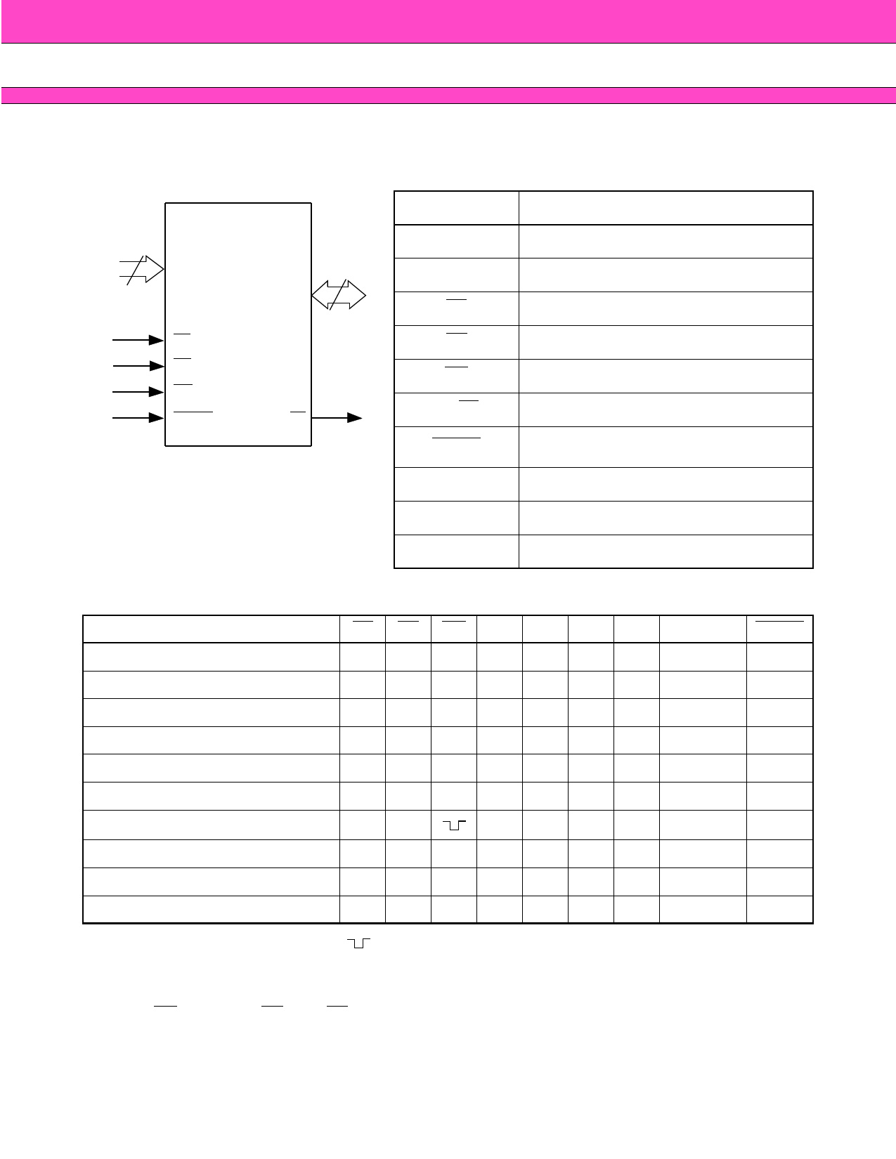
s LOGIC SYMBOL
22
A 0 to A 21
8
DQ0 to DQ7
CE
OE
WE
RESET
RY/BY
Table 1 MBM29F033C Pin Configuration
Pin
Function
A0 to A21
Address Inputs
DQ0 to DQ7
Data Inputs/Outputs
CE
Chip Enable
OE
Output Enable
WE
Write Enable
RY/BY
RESET
N.C.
Ready-Busy Output
Hardware Reset Pin/Sector Protection
Unlock
No Internal Connection
VSS
Device Ground
VCC
Device Power Supply
Table 2 MBM29F033C User Bus Operations
Operation
CE OE WE A0 A1 A6
Auto-Select Manufacturer Code (1)
L
L
H
L
L
L
Auto-Select Device Code (1)
L LHHL L
Read (2)
L
L
H
A0
A1
A6
Standby
HXXXXX
Output Disable
L HHX X X
Write
L
H
L
A0
A1
A6
Enable Sector Group Protection (3)
L
VID
XXX
Verify Sector Group Protection (3)
L LHLHL
Temporary Sector Group Unprotection X X X X X X
Reset (Hardware)
XXXXXX
A9 DQ0 to DQ7 RESET
VID
Code
H
VID
Code
H
A9
DOUT
H
X HIGH-Z
H
X HIGH-Z
H
A9
DIN
H
VID
X
H
VID
Code
H
X
X
VID
X HIGH-Z
L
Legend: L = VIL, H = VIH, X = VIL or VIH, = Pulse Input. See DC Characteristics for voltage levels.
Notes: 1. Manufacturer and device codes may also be accessed via a command register write sequence. Refer
to Tables 6.
2. WE can be VIL if OE is VIL, OE at VIH initiates the write operations.
3. Refer to the section on Sector Group Protection.
7
Share Link: 