TC1264 Просмотр технического описания (PDF) - Microchip Technology
Номер в каталоге
Компоненты Описание
Список матч
TC1264 Datasheet PDF : 12 Pages
| |||
TC1264
1.0 ELECTRICAL
CHARACTERISTICS
Absolute Maximum Ratings*
Input Voltage .........................................................6.5V
Output Voltage.................. (VSS – 0.3V) to (VIN + 0.3V)
Power Dissipation................Internally Limited (Note 8)
Maximum Voltage on Any Pin ........ VIN +0.3V to -0.3V
Operating Temperature Range...... -40°C < TJ < 125°C
Storage Temperature.......................... -65°C to +150°C
*Stresses above those listed under "Absolute Maximum
Ratings" may cause permanent damage to the device. These
are stress ratings only and functional operation of the device
at these or any other conditions above those indicated in the
operation sections of the specifications is not implied.
Exposure to Absolute Maximum Rating conditions for
extended periods may affect device reliability.
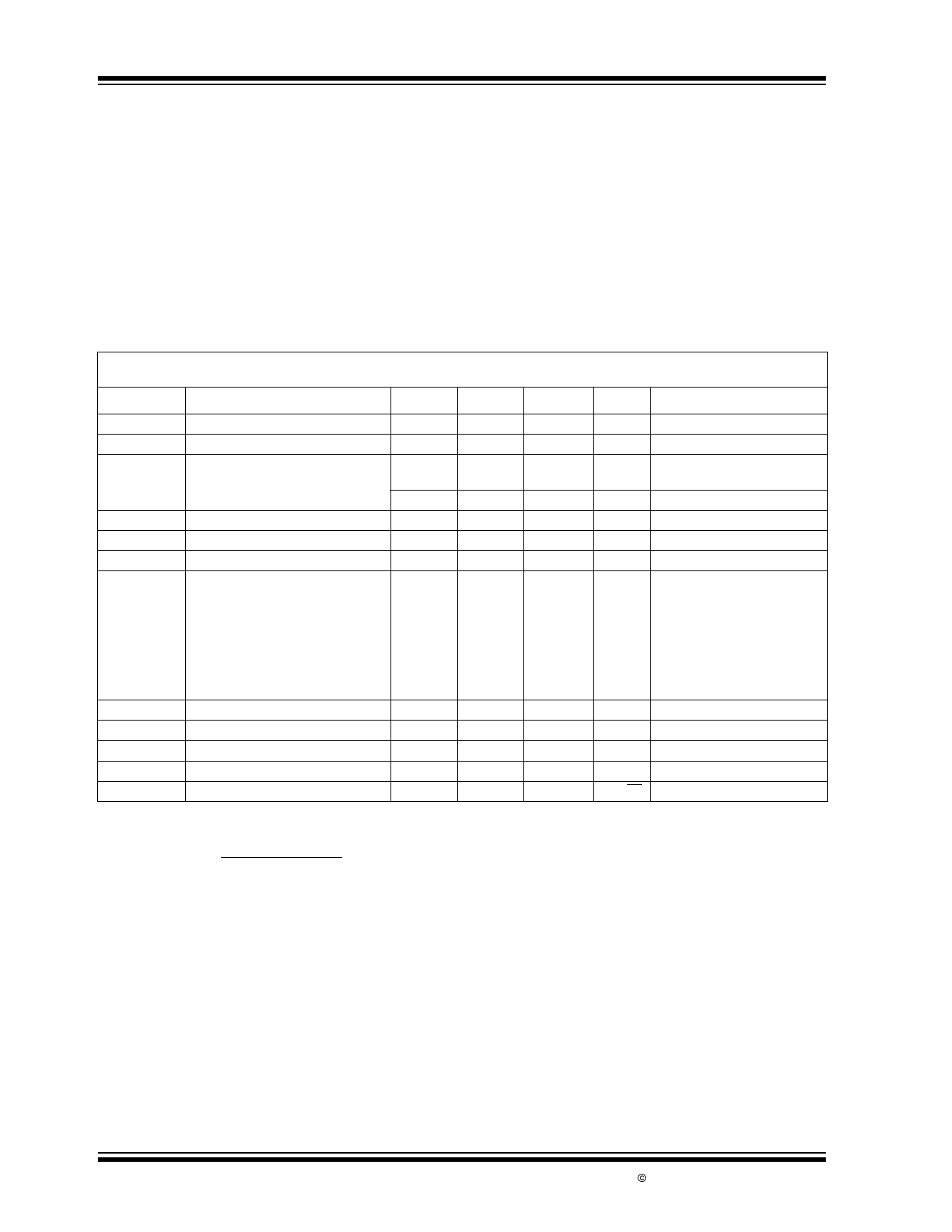
TC1264 ELECTRICAL SPECIFICATIONS
Electrical Characteristics: VIN = VR + 1.5V, (Note 1), IL = 100µA, CL = 3.3µF, TA = 25°C, unless otherwise noted. Boldface type
specifications apply for junction temperatures of -40°C to +125°C.
Symbol
Parameter
Min
Typ
Max
Units
Test Conditions
VIN
IOUTMAX
VOUT
Input Operating Voltage
Maximum Output Current
Output Voltage
∆VOUT/∆T
∆VOUT/∆VIN
∆VOUT/VOUT
VIN-VOUT
VOUT Temperature Coefficient
Line Regulation
Load Regulation
Dropout Voltage
2.7
—
6.0
800
—
—
VR – 2.5%
VR – 2%
VR – 7%
—
VR ± 0.5%
VR ± 0.5%
—
40
VR + 2.5%
VR + 3%
VR + 3%
—
—
0.007
0.35
-0.01
0.002
0
—
20
30
—
50
160
—
150
480
—
260
800
—
450
1300
—
700
1000
—
890
1400
V
mA
V
V
ppm/°C
%
%/mA
mV
Note 2
VR ≥ 2.5V
VR = 1.8V
IL = 0.1mA to 800mA (Note 3)
Note 4
(VR + 1V) ≤ VIN ≤ 6V
IL = 0.1mA to IOUTMAX (Note 5)
VR ≥ 2.5V, IL = 100µA
IL = 100mA
IL = 300mA
IL = 500mA
IL = 800mA
VR = 1.8V, IL = 500mA
IL = 800mA
(Note 6)
IDD
PSRR
Supply Current
Power Supply Rejection Ratio
—
80
130
µA IL = 0
—
64
—
dB F ≤ 1kHz
IOUTSC
Output Short Circuit Current
—
1200
—
mA VOUT = 0V
∆VOUT/∆PD Thermal Regulation
—
0.04
—
V/W Note 7
eN
Output Noise
—
260
—
nV/√Hz IL = IOUTMAX, F = 10kHz
Note
1: VR is the regulator output voltage setting.
2: The minimum VIN has to justify the conditions: VIN ≥ VR + VDROPOUT and VIN ≥ 2.7V for IL = 0.1mA to IOUTMAX.
3: This accuracy represents the worst case over the entire output current and temperature range.
4: TC VOUT = (VOUTMAX – VOUTMIN) x 106
VOUT x ∆T
5: Regulation is measured at a constant junction temperature using low duty cycle pulse testing. Load regulation is tested over a load range
from 0.1mA to the maximum specified output current. Changes in output voltage due to heating effects are covered by the thermal
regulation specification.
6: Dropout voltage is defined as the input to output differential at which the output voltage drops 2% below its nominal value measured at a
1.5V differential.
7: Thermal Regulation is defined as the change in output voltage at a time T after a change in power dissipation is applied, excluding load or
line regulation effects. Specifications are for a current pulse equal to ILMAX at VIN = 6V for T = 10 msec.
8: The maximum allowable power dissipation is a function of ambient temperature, the maximum allowable junction temperature and the
thermal resistance from junction-to-air (i.e., TA, TJ, θJA). Exceeding the maximum allowable power dissipation causes the device to initiate
thermal shutdown. Please see Section 4.0 Thermal Considerations for more details.
DS21375B-page 2
© 2002 Microchip Technology Inc.
Share Link: 