IDT71B74S12TP Просмотр технического описания (PDF) - Integrated Device Technology
Номер в каталоге
Компоненты Описание
Список матч
IDT71B74S12TP Datasheet PDF : 9 Pages
| |||
IDT71B74
BiCMOS STATIC RAM 64K (8K x 8-BIT) CACHE-TAG RAM
COMMERCIAL TEMPERATURE RANGE
AC ELECTRICAL CHARACTERISTICS (VCC = 5.0V ± 10%)
71B74S8 71B74S10 71B74S12 71B74S15
Symbol
Parameter
Min. Max. Min. Max. Min. Max. Min. Max.
Write Cycle
tWC
Write Cycle Time
8
— 10 — 12 — 15 —
tCW
Chip Select to End of Write
7
—
8
—
9
— 10 —
tAW
Address Valid to End of Write
7
—
8
—
9
— 10 —
tAS
Address Set-up Time
0
—
0
—
0
—
0
—
tWP
Write Pulse Width
7
—
8
—
9
— 10 —
tWR
tWHZ(1)
Write Recovery Time (CS, WE)
Write Enable to Output in High-Z
0
—
0
—
0
—
0
—
—
5
—
5
—
5
—
5
tDW
Data Valid to End of Write
5
—
5
—
6
—
8
—
tDH
tOW(1)
Data Hold from Write Time
Output Active from End of Write
0
—
0
—
0
—
0
—
2
—
2
—
2
—
2
—
NOTE:
1. This parameter is guaranteed with the AC Load (Figure 2) by device characterization, but is not production tested.
71B74S20
Min. Max. Unit
20 — ns
15 — ns
15 — ns
0
— ns
15 — ns
0
— ns
— 5 ns
10 — ns
0
— ns
2
— ns
3013 tbl 11
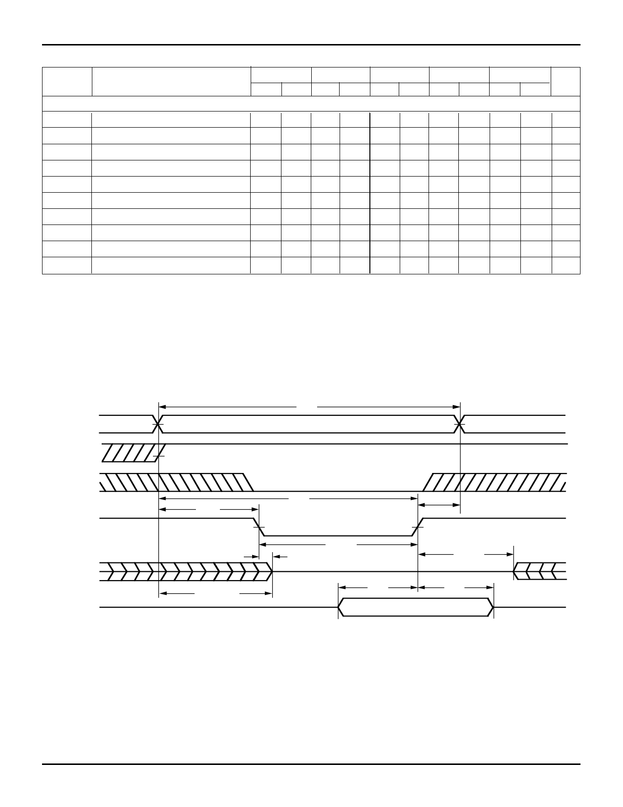
TIMING WAVEFORM OF WRITE CYCLE NO. 1 (WE Controlled Timing, OE HIGH During Write)(1, 6)
tWC
ADDRESS
OE
CS
t AW
t AS
t WR (3)
WE
t WHZ (8,9)
t WP (2)
t OW (9)
DATAOUT
DATAIN
t OHZ (4,9)
t DW
t DH
DATA VALID
NOTES:
3013 drw 11
1. , WE CS must be inactive during all address transitions.
2. A write occurs during the overlap of a LOW WE and a LOW CS.
3. tWR is measured from the earlier of CS or WE going HIGH to the end of the write cycle.
4. During this period, I/O pins are in the output state and input signals must not be applied.
5. If the CS LOW transition occurs simultaneously with or after the WE LOW transition, the outputs remain in a high-impedance state.
6. OE is continuously HIGH, OE ≥ VIH. If during the WE controlled write cycle the OE is LOW, tWP must be greater or equal to tWHZ + tDW to allow the I/O
drivers to turn off and the data to be placed on the bus for the required tDW. If OE is HIGH during the WE controlled write cycle, this requirement does not
apply and the minimum write pulse is the specified tWP. For a CS controlled write cycle, OE may be LOW with no degradation to tCW timing.
7. DATAOUT is never enabled, therefore the output is in High-Z state during the entire write cycle.
8. tWHZ is not included if OE remains HIGH during the write cycle. If OE is LOW during the Write Enabled write cycle then tWHZ must be added to tWP and tCW.
9. Transition is measured ±200mV from steady state.
14.1
6
Share Link: 