MC14511B Просмотр технического описания (PDF) - Motorola => Freescale
Номер в каталоге
Компоненты Описание
Список матч
MC14511B Datasheet PDF : 9 Pages
| |||
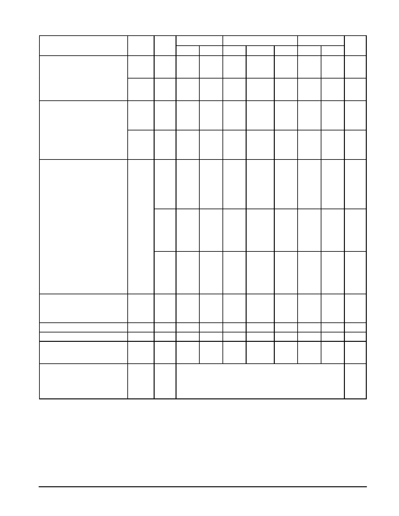
ÎÎÎÎEÎÎÎÎLEÎÎÎÎCTRÎÎÎÎICAÎÎÎÎL CÎÎÎÎHAÎÎÎÎRACÎÎÎÎTEÎÎÎÎRISÎÎÎÎTICÎÎÎÎS (VÎÎÎÎoltagÎÎÎÎesVRÎÎÎÎDefDeÎÎÎÎrencÎÎÎÎedtoÎÎÎΖV5S5ÎÎÎÎS_C) ÎÎÎÎÎÎÎÎÎÎÎÎÎÎÎÎÎÎÎÎ25_ÎÎÎÎC ÎÎÎÎÎÎÎÎÎÎÎÎÎÎÎÎÎÎÎÎ125ÎÎÎÎ_C ÎÎÎÎÎÎÎÎÎÎÎÎÎÎÎÎ
Characteristic
Symbol Vdc
Min
Max
Min
Typ #
Max
Min
Max Unit
Output Voltage
Vin = VDD or 0
“0” Level VOL
5.0
—
0.05
—
10
—
0.05
—
15
—
0.05
—
0
0.05
—
0.05 Vdc
0
0.05
—
0.05
0
0.05
—
0.05
Vin = 0 or VDD
“1” Level VOH
5.0
4.1
—
4.1
4.57
—
4.1
—
Vdc
10
9.1
—
9.1
9.58
—
9.1
—
15
14.1
—
14.1
14.59
—
14.1
—
Input Voltage #
“0” Level VIL
Vdc
(VO = 3.8 or 0.5 Vdc)
5.0
—
1.5
—
2.25
1.5
—
1.5
(VO = 8.8 or 1.0 Vdc)
10
—
3.0
—
4.50
3.0
—
3.0
(VO = 13.8 or 1.5 Vdc)
15
—
4.0
—
6.75
4.0
—
4.0
“1” Level VIH
Vdc
(VO = 0.5 or 3.8 Vdc)
5.0
3.5
—
3.5
2.75
—
3.5
—
(VO = 1.0 or 8.8 Vdc)
10
7.0
—
7.0
5.50
—
7.0
—
(VO = 1.5 or 13.8 Vdc)
15
11
—
11
8.25
—
11
—
Output Drive Voltage
VOH
Vdc
(IOH = 0 mA)
Source
5.0
4.1
—
4.1
4.57
—
4.1
—
(IOH = 5.0 mA)
—
—
—
4.24
—
—
—
(IOH = 10 mA)
3.9
—
3.9
4.12
—
3.5
—
(IOH = 15 mA)
—
—
—
3.94
—
—
—
(IOH = 20 mA)
3.4
—
3.4
3.70
—
3.0
—
(IOH = 25 mA)
—
—
—
3.54
—
—
—
(IOH = 0 mA)
(IOH = 5.0 mA)
(IOH = 10 mA)
(IOH = 15 mA)
(IOH = 20 mA)
(IOH = 25 mA)
10
9.1
—
9.1
9.58
—
9.1
—
Vdc
—
—
—
9.26
—
—
—
9.0
—
9.0
9.17
—
8.6
—
—
—
—
9.04
—
—
—
8.6
—
8.6
8.90
—
8.2
—
—
—
—
8.70
—
—
—
(IOH = 0 mA)
(IOH = 5.0 mA)
(IOH = 10 mA)
(IOH = 15 mA)
(IOH = 20 mA)
(IOH = 25 mA)
Output Drive Current
(VOL = 0.4 V)
(VOL = 0.5 V)
(VOL = 1.5 V)
IOL
Sink
Input Current
Iin
Input Capacitance
Cin
Quiescent Current
IDD
(Per Package) Vin = 0 or VDD,
Iout = 0 µA
Total Supply Current**†
IT
(Dynamic plus Quiescent,
Per Package)
(CL = 50 pF on all outputs, all
buffers switching)
15
14.1
—
14.1
14.59
—
14.1
—
Vdc
—
—
—
14.27
—
—
—
14
—
14
14.18
—
13.6
—
—
—
—
14.07
—
—
—
13.6
—
13.6
13.95
—
13.2
—
—
—
—
13.70
—
—
—
5.0
0.64
—
0.51
0.88
10
1.6
—
1.3
2.25
15
4.2
—
3.4
8.8
mAdc
—
0.36
—
—
0.9
—
—
2.4
—
15
—
± 0.1
— ± 0.00001 ± 0.1
—
± 1.0 µAdc
—
—
—
—
5.0
7.5
—
—
pF
5.0
—
5.0
—
0.005
5.0
—
150 µAdc
10
—
10
—
0.010
10
—
300
15
—
20
—
0.015
20
—
600
5.0
IT = (1.9 µA/kHz) f + IDD
µAdc
10
IT = (3.8 µA/kHz) f + IDD
15
IT = (5.7 µA/kHz) f + IDD
#Noise immunity specified for worst–case input combination.
Noise Margin for both “1” and “0” level =
1.0 Vdc min @ VDD = 5.0 Vdc
2.0 Vdc min @ VDD = 10 Vdc
2.5 Vdc min @ VDD = 15 Vdc
**āThe formulas given are for the typical characteristics only at 25_C.
†To calculate total supply current at loads other than 50 pF:
IT(CL) = IT(50 pF) + 3.5 x 10⁻³ (CL – 50) VDDf
where: IT is in µA (per package), CL in pF, VDD in Vdc, and f in kHz is input frequency.
MC14511B
362
MOTOROLA CMOS LOGIC DATA
Share Link: 