SPX3819M5-1.2/TR Просмотр технического описания (PDF) - Signal Processing Technologies
Номер в каталоге
Компоненты Описание
Список матч
SPX3819M5-1.2/TR Datasheet PDF : 12 Pages
| |||
Power Dissipation ...................................................... Internally Limited
Lead Temp. (Soldering, 5 Seconds) ........................................... 260°C
Operating Junction Temperature Range ................... -40°C to +125°C
Input Supply Voltage ........................................................ -20V to +20V
Enable Input Voltage ........................................................ -20V to +20V
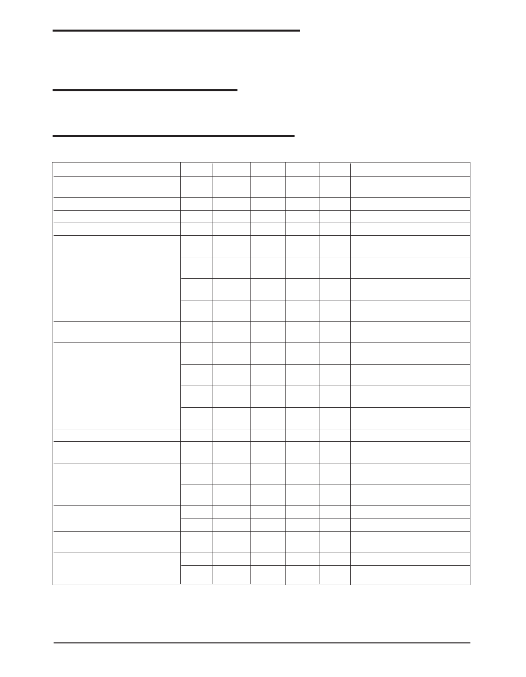
ABSOLUTE MAXIMUM RATINGS
RECOMMENDED OPERATIONG CONDITIONS
Input Voltage ................................................................... +2.5V to+16V
Operating Junction Temperature Range ................... -40°C to +125°C
Enable Input Voltage .............................................................. 0V to VIN
ELECTRICAL CHARACTERISTICS
TJ=25°C, VOUT + 1V, for 1.2V Option VIN=VOUT + 1.2V IL=100µA, CL=1µF, and VENABLE ≥ 2.4V. The ♦ denotes the
specifications which apply over full operating temperature range -40°C to +85°C, unless otherwise specified.
PARAMETER
MIN
TYP
MAX UNITS
♦ CONDITIONS
Output Voltage Tolerance
-1
-2
+1
%
+2
♦
Output Voltage Temperature Coef.
Line Regulation
Load Regulation
Dropout Voltage
(VIN-VO)(Note 2)
57
ppm/°C
0.04
0.1
%/V
VIN=VOUT + 1V to 16V
0.05
0.4
%
IL = 0.1mA to 500mA
10
60
mV
IL = 100µA
80
♦
125
175
mV
250
IL = 50mA
♦
180
350
mV
450
IL = 150mA
♦
340
550
mV
700
IL = 500mA
♦
Quiescent Current (IGND)
Ground Pin Current (IGND)
0.05
3
µA
8
90
150
µA
190
VENABLE ≤ 0.4V
♦
VENABLE ≤ 0.25V
IL = 100µA
♦
250
650
µA
900
IL = 50mA
♦
Ripple Rejection (PSRR)
1.0
2.0
mA
2.5
6.5
25.0
mA
30.0
70
dB
IL = 150mA
♦
IL = 500mA
♦
Current Limit (ILIMIT)
800
mA
950
VOUT = 0V
♦
Output Noise (eNO)
300
µVRMS
IL=10mA, CL=1.0µF, CIN=1µF,
(10Hz-100kHz)
Input Voltage Level Logic Low (VIL)
Input Voltage Level Logic High (VIH)
ENABLE Input Current
Thermal Resistance (Note 1)
40
µVRMS
IL=10mA, CL=10µF, CBYP =1µF,
CIN =1µF, (10Hz-100kHz)
0.4
V
OFF
2
V
ON
0.01
2
µA
3
20
VIL ≤ 0.4V
VIH ≥ 2.0V
220
°C/W
♦ SOT-23-5 / Junction to Ambient
180
°C/W
♦ SO-8 / Junction to Ambient
NOTES
Note 1: The maximum allowable power dissipation is a function of maximum operating junction temperature, TJ(max) the junction to ambient thermal
resistance, and the ambient θJA, and the ambient temperature TA. The maximum allowable power dissipation at any ambient temperature is
given: PD(max) = (TJ(max)-TA)/θJA, exceeding the maximum allowable power limit will result in excessive die temperature; thus, the regulator will
go into thermal shutdown. The θJA of the SPX3819 is 220°C/W mounted on a PC board.
Note 2: Not applicable to output voltage 2V or less.
Date:6/8/2004
SPX3819 500mA, Low Noise LDO Voltage Regulator
2
© Copyright 2004 Sipex Corporation
Share Link: 