SPX1202M3-1.5 Просмотр технического описания (PDF) - Signal Processing Technologies
Номер в каталоге
Компоненты Описание
Список матч
SPX1202M3-1.5 Datasheet PDF : 5 Pages
| |||
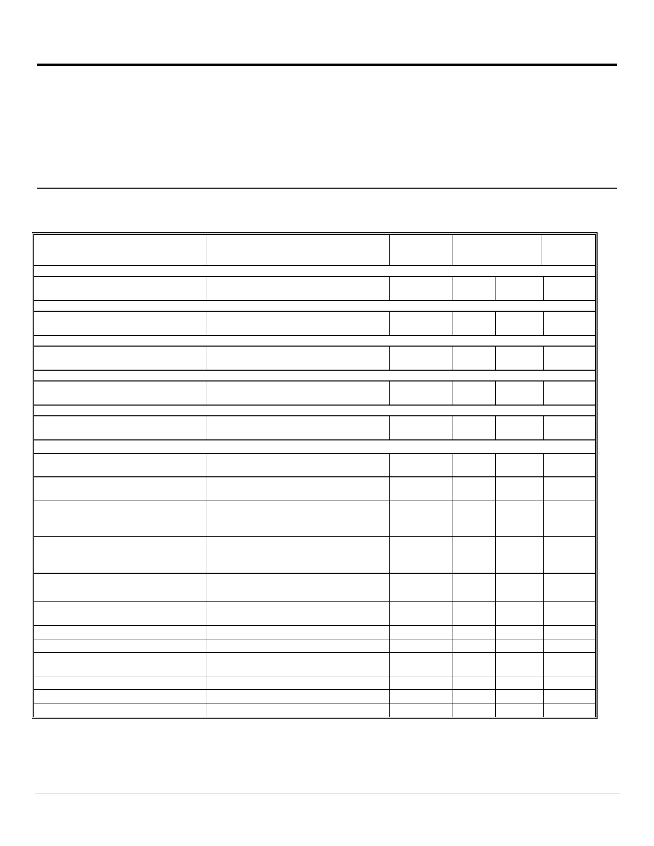
ABSOLUTE MAXIMUM RATINGS
Power Dissipation..........................................Internally Limited
Lead Temp. (Soldering, 5 Seconds) ................................ 260°C
Storage Temperature Range ............................ -65° to +150°C
Operating Junction Temperature Range
SPX1202................................................ -40C° to +125°C
SPX1202
Input Supply Voltage ......................................-20V to +20V
ESD Rating ............................................................2KV Min
ELECTRICAL CHARACTERISTICS at VIN = VOUT +1, Ta=25°C, CL =3.3µf, unless otherwise specified. Limits in
Boldface apply over the full operating temperature range.
Parameter
Conditions
SPX1202
Typ
Min
Max Units
1.5V Version
Output Voltage
2.5V Version
Output Voltage
3.0V Version
Output Voltage
3.3 V Version
Output Voltage
5.0V Version
Output Voltage
All Output Voltage
IOUT=10mA, VIN=5.00V
0≤IOUT≤600mA, 4.50≤VIN≤10V
IOUT=10mA, VIN=5.00V
0≤IOUT≤600mA, 4.50≤VIN≤10V
IOUT=10mA, VIN=5.00V
0≤IOUT≤600mA, 4.50≤VIN≤10V
IOUT=10mA, VIN=5.00V
0≤IOUT≤600mA, 4.50≤VIN≤10V
IOUT=10mA, VIN=5.00V
0≤IOUT≤600mA, 4.50≤VIN≤10
1.500
1.485
1.515
V
1.470
1.530
2.500
2.475
2.525
V
2.450
2.550
3.000
2.970
3.030
V
2.940
3.060
3.300
3.267
3.333
V
3.234
3.366
5.000
4.950
5.050
V
4.900
5.100
Reference Voltage
Output Voltage
Temperature Stability
Line Regulation
Load Regulation
Dropout Voltage
( Note 2)
IOUT=10mA, (VIN- VIN) =2V
10≤IOUT≤600mA, 1.4≤(VIN -VIN) ≤10V
(Note 1)
4.50V ≤VIN≤12V, VOUT=3.00, IOUT=0
4.80V ≤VIN≤12V, VOUT=3.30, IOUT=0
6.50V ≤VIN≤15V, VOUT=5.00, IOUT=0
0≤IOUT≤600mA, VIN=4.50V, VOUT=3.00
0≤IOUT≤600mA, VIN=4.80V, VOUT=3.30
0≤IOUT≤600mA, VIN=6.50V, VOUT=5.00
IL = 100mA
IL = 600mA
1.250
1.238
1.262
V
1.225
1.270
0.05
%
1.00
7.00
mV
1.00
7.00
1.00
10.00
1.00
12.00
mV
1.00
12.00
1.00
15.00
1.00
1.10
V
1.05
1.15
Quiescent Current
4.25V ≤VIN≤6.5V
5.00
10.00
mA
Current Limit
Thermal Regulation
Ripple Rejection
Long Term Stability
RMS Output Noise
Thermal Resistance
(VIN-VOUT)=5V
850
25°°C,30mS Pulse
0.01
fRIPPLE=120Hz, (VIN-VOUT) = 3V,
60
VRIPPLE=1Vp-p
125°C, 1000Hrs
% of VOUT, 10Hz≤f≤10kHz
Junction to case, at tab
1000
0.1
75
0.03
0.003
15
mA
%/W
dB
%
%
°C/W°
Note 1: Output temperature coefficient is defined as the worst case voltage change divided by the total temperature range
Note 2: Dropout voltage is defined as the input to output differential at which the output voltage drops 100mV below its nominal value measured at 1V differential at
very low values of programmed output voltage, the minimum input supply voltage of 2V ( 2.3V over temperature) must be taken into account.
Note 3: Thermal regulation is defined as the change in output voltage at a time T after a change in power dissipation is applied. excluding loads or line
regulation effect
Rev. 10/19/00
Share Link: 