AN7820 Просмотр технического описания (PDF) - Fairchild Semiconductor
Номер в каталоге
Компоненты Описание
Список матч
AN7820 Datasheet PDF : 17 Pages
| |||
POWER SUPPLIES
EB7820/24 requires four power supply sources: analog -
5.2 V (-A5.2 V), analog +5 V (+A5 V), digital - 5.2 V (- D5.2
V), and digital +5 V (+D5 V) . P1 is the power connector. (See
figure 2.) The recommended operating voltage range is
shown in table 1.
Table 1 - Recommended Power Supply Operating Range
Typ
PS
Min
Typ
Max
Current
-A5.2 V -4.95 V -5.20 V - 5.45 V
60 mA
+A5 V +4.75 V +5.00 V +5.25 V
240 mA
-D5.2 V -4.95 V -5.20 V - 5.45 V
15 mA
+D5 V +4.75 V +5.00 V +5.25 V
60 mA
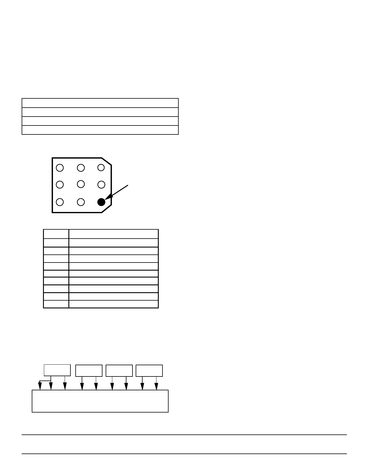
Figure 2 - P1, Power Supply Connector’s Pin Assignment
9
6
3
8
5
2
7
4
1
FEMALE
TERMINAL
P1 (top view)
PIN#
1
2
3
4
5
6
7
8
9
PIN ASSIGNMENT
ANALOG - 5.2 V
ANALOG - 5.2 V RETURN # 1 (AGND)
ANALOG - 5.2 V RETURN # 2 (AGND)
ANALOG + 5V
ANALOG + 5 V RETURN (AGND)
DIGITAL - 5.2 V RETURN (DGND)
DIGITAL + 5 V
DIGITAL + 5 V RETURN (DGND)
DIGITAL - 5.2 V
The total power dissipation is typically 1.89 watts, including
the SPT7820 or SPT7824 (1.1 W typ).
POWER SUPPLY HOOK-UPS
Figure 3 - P1 Connector/Hook-Up
+ -5.2 V-
+ + 5 V - +- 5.2 V- + + 5 V -
23 1
45 69
78
P1 POWER CONNECTOR
POWER SUPPLIES AND GROUNDING
The SPT7820/24 requires two analog supply voltages: -
A5.2 V and +A5 V. The +A5 V supply is common to analog
VCC (pin 18 &25) and digital DVCC (pin 14 and 28). A ferrite
bead in series with each supply (RF1 and RF2) reduces the
transient noise injected into VCC. The bead (RF1 or RF2) to
SPT7820/24 connections should not be shared with any
other device. Bypass each power supply pin as closely as
possible to the device (0.1 µF to AGND for each VEE and
VCC pin and 0.01 µF to DGND for the DVCC pin).
AGND and DGND are isolated on the SPT7820 and SPT7824.
Both -A5.2 V and +A5 V are the analog supply sources. As
in most very high speed ADCs, grounding is critical. There-
fore, the ground plane technique is the most desirable for the
SPT7820/24. To accomplish this, split and tie together the
AGND and DGND ground planesonly at the device (SPT7820/
24) through an RF bead. The EB7820/24 is a four-layer
printed circuit board: the top signal, ground (AGND & DGND)
plane, power plane and the bottom signal. The two ground
planes are connected together at the device through a ferrite
bead (RF3). All three ferrite beads (RF1-3) are located close
to the ADC.
The analog input (pin 21) is physically sandwiched between
the reference taps. Carefully plan printed circuit board layout
to minimize any pick-up from VIN (high frequency) into the
references (VFT or VFB).
REFERENCE CIRCUIT
The SPT7820/24 requires the use of two voltage references:
VFT and VFB. VFT is the force for the top of the voltage
reference ladder (+2.5 V typ), and VFB (-2.5 V typ) is the force
for the bottom of the voltage reference ladder. Both voltages
are applied across an internal reference ladder resistance of
900 Ω. In addition, there are three reference ladder taps:
VST, VRM and VSB. VST is the top of the reference ladder
tap (+2 V), VRM is the middle point (0.0 V typ), and VSB is the
bottom of the reference ladder tap (-2 V). The voltages seen
at VST and VSB are the expected full scale input voltages of
the device when VFT and VFB are driven to the recom-
mended voltages (+2.5 V and -2.5 V respectively). Use VST
and VSB to monitor the actual full scale input voltages (±2 V)
by adjusting VFT and VFB. These adjustments have some
interaction; repeat a few times as needed until VST and VSB
settle at the desired voltages. Do not drive VRM as is
commonly done with a standard flash ADC converter. When
not being used (VST, VRM & VSB), decouple with a 0.01 µF
chip capacitor (surface mounted) to AGND from each tap to
minimize high frequency noise injection.
Referring to figure 17, U2 is the + 2.5 V reference with
±150 mV of adjustable range (R1 potentiometer). U3 (OP-
-07) is an inverting amplifier. Its tolerance is 5% with ±300 mV
of adjustable range (R2 potentiometer). Fairchild recom-
AN7820/24
2
5/22/97
Share Link: 