SP6832EK Просмотр технического описания (PDF) - Signal Processing Technologies
Номер в каталоге
Компоненты Описание
Список матч
SP6832EK Datasheet PDF : 15 Pages
| |||
PINOUT
VOUT 1
VIN 2
C1- 3
SP6832
5 C1+
4 GND
PIN ASSIGNMENTS
Pin 1— VOUT — Inverting charge pump output.
Pin 2 — VIN — Input to the positive power
supply.
Pin 3 — C1- — Negative terminal to the charge
pump capacitor.
Pin 4 — GND — Ground reference.
Pin 5 — C1+ — Positive terminal to the charge
pump capacitor.
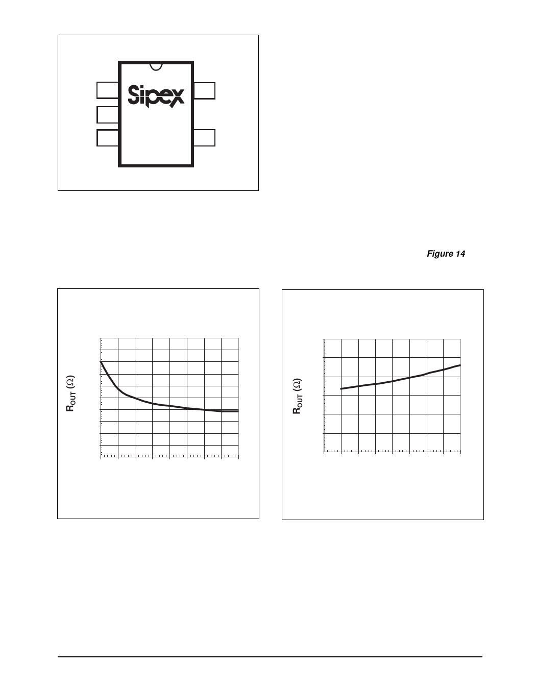
TYPICAL PERFORMANCE CHARACTERISTICS
V
IN
=
+5.0V,
C1
=
C2
=
C3
=
0.33µF
and
T
AMB
=
25oC
unless
otherwise
noted.
The
circuit
found
in
Figure
14
was
used to obtain the following typical performance characteristics (unless otherwise noted).
50
45
40
35
30
25
20
15
10
5
0
1.5 2 2.5 3 3.5 4 4.5 5 5.5
(V)
30
25
20
15
10
5
0
-60 -40 -20 0 20 40 60 80 100
temperature OC
Figure 1. Output Resistance vs. Supply Voltage with
a 5mA load
Figure 2. Output Resistance vs. Temperature with
a 25mA load
SP6832DS/04
SP6832 High Speed, High Efficiency Voltage Inverter
3
© Copyright 2000 Sipex Corporation
Share Link: 