ICS9248F-153-T Просмотр технического описания (PDF) - Integrated Circuit Systems
Номер в каталоге
Компоненты Описание
Список матч
ICS9248F-153-T Datasheet PDF : 14 Pages
| |||
ICS9248-153
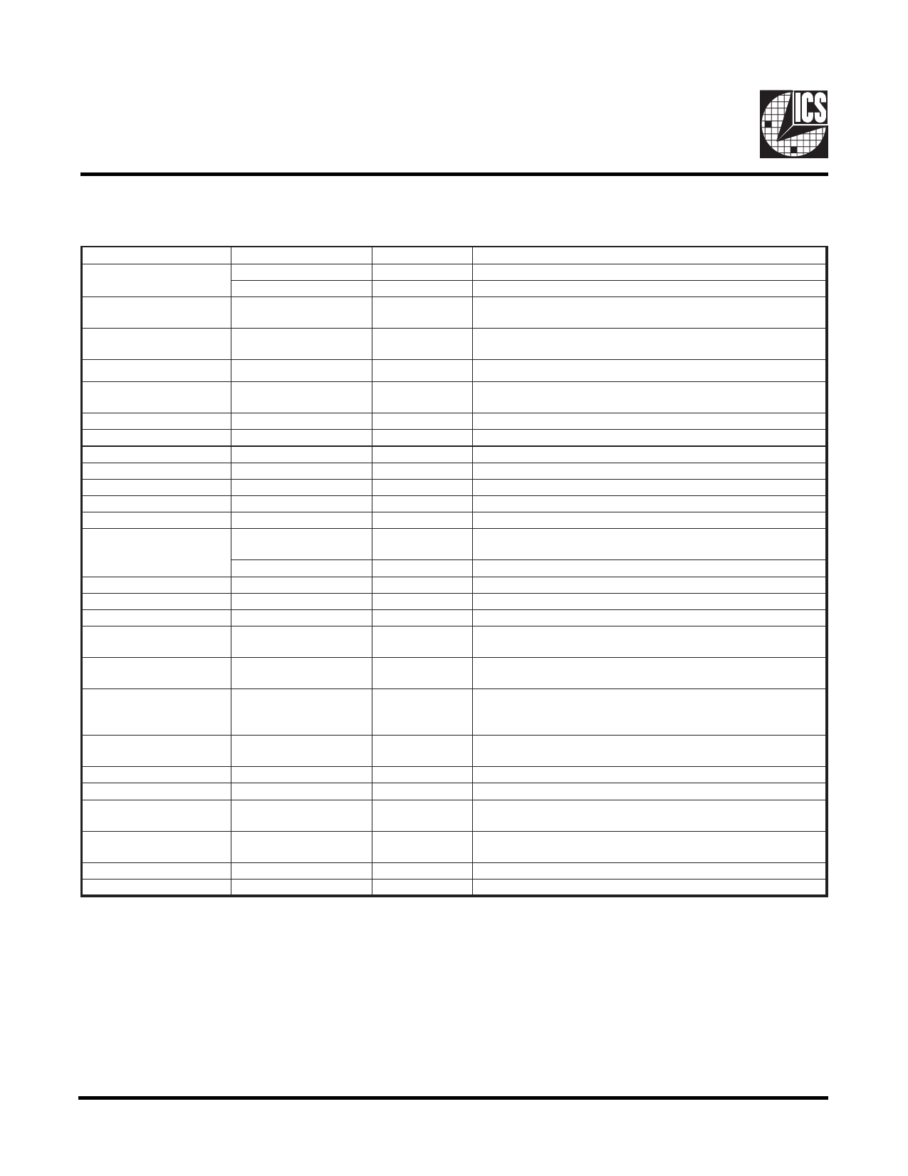
Pin Descriptions
PIN NUMBER
2,1
3, 6, 21, 25,
33, 38, 41, 47
4
5
7
17, 16, 14, 13, 11, 10, 8
9, 15
18
20, 19
34
22
23
24
26
27
28
29
30
PIN NAME
FS (1:0)
REF (1:0)
GND
X1
X2
PCICLK_F
PCICLK (6:0)
VDDPCI
VDDAGP
AGP (1:0)
VDD
VDD48
48MHz
SEL24-48#
24-48MHz
SCLK
SDATA
FS2
SPREAD#
PD#
31
CPU_STOP#
32
46
35, 44
42, 39, 36
43, 40, 37
45
48
PCI_STOP#
SDRAM_OUT
RESERVED
CPUCLKT (2:0)
CPUCLKC (2:0)
VDDSD
VDDREF
TYPE
IN
OUT
PWR
IN
OUT
OUT
OUT
PWR
PWR
OUT
PWR
PWR
OUT
IN
OUT
IN
I/O
IN
IN
IN
IN
IN
OUT
N/C
OUT
OUT
PWR
PWR
DESCRIPTION
Frequency Select pins, has pull-up to VDD
14.318MHz clock output
Ground
XTAL_IN 14.318MHz Crystal input, has internal 33pF load
cap and feed back resistor from X2
XTAL_OUT Crystal output, has internal load cap 33pF
Free Running PCI output. Not affected by the PCI_STOP#
input.
PCI clock outputs. TTL compatible 3.3V
Power for PCICLK outputs, nominally 3.3V
Power for AGP outputs, nominally 3.3V
AGP outputs defined as 2X PCI. These may not be stopped.
Isolated power for core, nominally 3.3V
Power for 48MHz and 24MHz outputs nominally 3.3V
48MHz output
Selects 24 or 48MHz output for pin 24
Low = 48MHz High = 24MHz
Fixed clock out selectable through SEL24-48#
Clock pin of I2C circuitry 5V tolerant
Data pin for I2C circuitry 5V tolerant
Frequency Select pin, has pull-up to VDD
Enables Spread Spectrum feature when LOW. Center spread of
+/- 0.25%.
Powers down chip, active low. Internal PLL & all outputs
are disabled.
Halts CPUCLKs. CPUCLKT is driven LOW wheras
CPUCLKC is driven HIGH when this pin is asserted
(Active LOW).
Halts PCI Bus at logic "0" level when driven low. PCICLK_F
is not affected by this pin
Reference clock for SDRAM zero delay buffer
Future CPU power rail
"True" clocks of differential pair CPU outputs. These open
drain outputs need an external 1.5V pull-up.
"Complementory" clocks of differental pair CPU output. These
open drain outputs need an external 1.5V pull_up.
Power for SDRAM_OUT pin. Norminally 3.3V
Power for REF, X1, X2, nominally 3.3V
Third party brands and names are the property of their respective owners.
2
Share Link: 