RT9227ACS Просмотр технического описания (PDF) - Richtek Technology
Номер в каталоге
Компоненты Описание
Список матч
RT9227ACS Datasheet PDF : 10 Pages
| |||
RT9227A
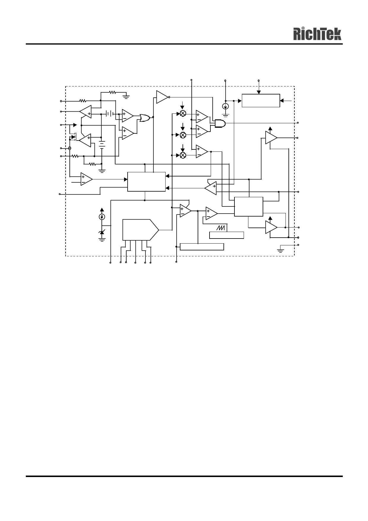
Function Block Diagram
Preliminary
VSEN1
OCSET1
VCC
VSEN3
GATE3
VIN2
VOUT2
FB2
FAULT
_
3.3V
0.3V
_
1.26V
110%
90%
L IN EAR
UN DER
VOLTAGE LUV
115%
200µA
POWER-ON 3.3V
RESET (POR)
VCC
OC2
0.25A
VCC
11µA
5V
0V
SOFT-START
& FAULT
LOGIC
OC1 _
UPPER
DRIVE
INHIBIT
DACOUT
TTL D/A
CONVERTER
(DAC)
GATE
PWM
CONTROL
LOGIC
ERROR
AMP
PWM COMP
OSCILLATOR
LOWER
DRIVE
COMPENSATION
VCC
PGOOD
UGATE1
PHASE1
LGATE1
PGND
GND
SS VID0 VID2 VID4
FB1
VID1 VID3
Functional Pin Description
VCC (Pin 1)
Provide a 12V bias supply for the IC to this pin. This
pin also provides the gate bias charge for all the
MOSFETs controlled by the IC.
VID0, VID1, VID2, VID3, VID4 (Pin 6, 5, 4, 3, and 2)
VIDO-4 are the input pins to the 5-bit DAC. The
states of these five pins program the internal voltage
reference, DACOUT. The level of DACOUT sets the
core converter output voltage. It also sets the core
PGOOD and OVP thresholds. Table 1 specifies the
DACOUT voltage of 32 combinations of VID levels.
PGOOD (Pin 7)
PGOOD is an open collector output used to indicate
the status of the output voltage. This pin is pulled low
www.richtek-ic.com.tw
4
when the core output is not within ±10% of the
DACOUT reference voltage and the other outputs are
below their under-voltage thresholds.
The PGOOD output is open for ‘11111’ VID codes
that inhibit operation. See table 1.
FAULT (Pin 8)
This pin is low during normal operation, but it is
pulled to about 8V (VCC = 12V) in the event of an
over-voltage or over-current condition.
SS (Pin 9)
Connect a capacitor from this pin to ground. This
capacitor, along with an internal 11µA (VSS >1V)
current source, sets the soft-start interval of the
converter.
DS9227A-02 July 2001
Share Link: 