HIP6019 Просмотр технического описания (PDF) - Intersil
Номер в каталоге
Компоненты Описание
Список матч
HIP6019 Datasheet PDF : 15 Pages
| |||
HIP6019
∆VOSC
OSC
PWM
COMP
-
+
DRIVER
DRIVER
ZFB
VE/A
-
ZIN
+
ERROR
AMP
REFERENCE
VIN
LO
VOUT
PHASE
CO
ESR
(PARASITIC)
DETAILED FEEDBACK COMPENSATION
C2
C1 R2
ZFB
VOUT
ZIN
C3 R3
R1
COMP
-
FB
+
HIP6019
REFERENCE
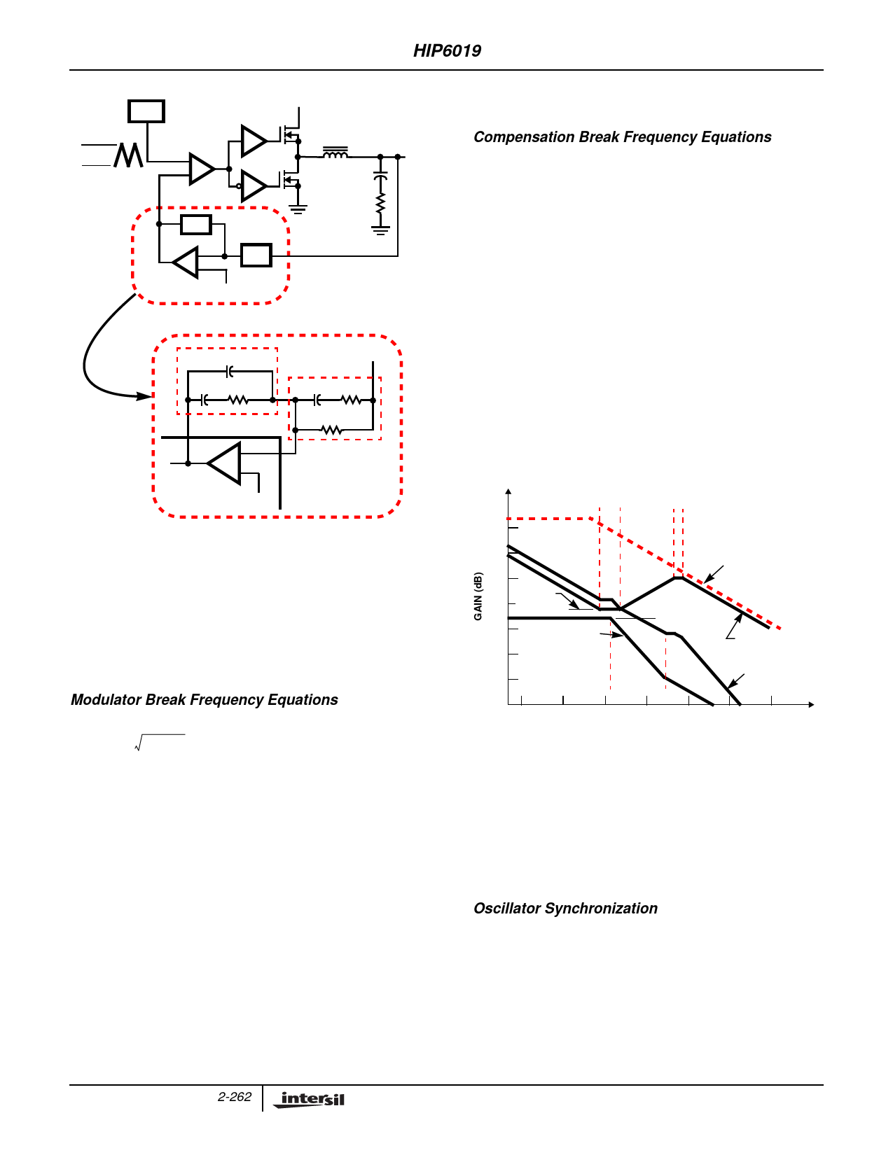
FIGURE 11. VOLTAGE-MODE BUCK CONVERTER COMPEN-
SATION DESIGN
The modulator transfer function is the small-signal transfer
function of VOUT/VE/A. This function is dominated by a DC
gain and the output filter, with a double pole break frequency
at FLC and a zero at FESR. The DC gain of the modulator is
simply the input voltage, VIN, divided by the peak-to-peak
oscillator voltage, ∆VOSC.
Modulator Break Frequency Equations
FLC=
-------------------1--------------------
2π × LO × CO
FESR= 2----π-----×-----E----S--1---R------×-----C----O---
The compensation network consists of the error amplifier
internal to the HIP6019 and the impedance networks ZIN
and ZFB. The goal of the compensation network is to
provide a closed loop transfer function with an acceptable
0dB crossing frequency (f0dB) and adequate phase margin.
Phase margin is the difference between the closed loop
phase at f0dB and 180 degrees. The equations below relate
the compensation network’s poles, zeros and gain to the
components (R1, R2, R3, C1, C2, and C3) in Figure 11.
Use these guidelines for locating the poles and zeros of the
compensation network:
1. Pick Gain (R2/R1) for desired converter bandwidth.
2. Place 1ST Zero below filter’s Double Pole (~75% FLC).
3. Place 2ND Zero at filter’s Double Pole.
4. Place 1ST Pole at the ESR Zero.
5. Place 2ND Pole at half the switching frequency.
6. Check Gain against Error Amplifier’s Open-Loop Gain.
7. Estimate Phase Margin - repeat if necessary.
Compensation Break Frequency Equations
FZ1 = 2----π-----×-----R---1--2-----×----C-----1--
FZ2 = 2----π-----×-----(--R-----1-----+-1----R-----3----)---×-----C-----3-
FP1
=
---------------------------1---------------------------
2π
×
R2
×
C-C----11-----+×-----CC-----22--
FP2 = 2----π-----×-----R---1--3-----×----C-----3--
Figure 12 shows an asymptotic plot of the DC-DC
converter’s gain vs frequency. The actual modulator gain has
a peak due to the high Q factor of the output filter at FLC,
which is not shown in Figure 12. Using the above guidelines
should yield a compensation gain similar to the curve
plotted. The open loop error amplifier gain bounds the
compensation gain. Check the compensation gain at FP2
with the capabilities of the error amplifier. The closed loop
gain is constructed on the log-log graph of Figure 12 by
adding the modulator gain (in dB) to the compensation gain
(in dB). This is equivalent to multiplying the modulator
transfer function to the compensation transfer function and
plotting the gain.
100
FZ1 FZ2 FP1 FP2
80
OPEN LOOP
60
ERROR AMP GAIN
40
20LOG
20 (R2/R1)
0
MODULATOR
-20
GAIN
20LOG
(VIN/∆VOSC)
COMPENSATION
GAIN
-40
FLC
FESR
CLOSED LOOP
GAIN
-60
10
100
1K
10K 100K 1M 10M
FREQUENCY (Hz)
FIGURE 12. ASYMPTOTIC BODE PLOT OF CONVERTER GAIN
The compensation gain uses external impedance networks
ZFB and ZIN to provide a stable, high bandwidth loop. A
stable control loop has a 0dB gain crossing with
-20dB/decade slope and a phase margin greater than 45
degrees. Include worst case component variations when
determining phase margin.
Oscillator Synchronization
The PWM controllers use a triangle wave for comparison with
the error amplifier output to provide a pulse-width modulated
wave. Should the output voltages of the two PWM converters
be programmed close to each other, then cross-talk could
cause nonuniform PHASE pulse-widths and increased output
voltage ripple. The HIP6019 avoids this problem by
synchronizing the two converters 180° out-of-phase for DAC
2-262
Share Link: 