SL74HC373 Просмотр технического описания (PDF) - System Logic Semiconductor
Номер в каталоге
Компоненты Описание
Список матч
SL74HC373 Datasheet PDF : 5 Pages
| |||
SL74HC373
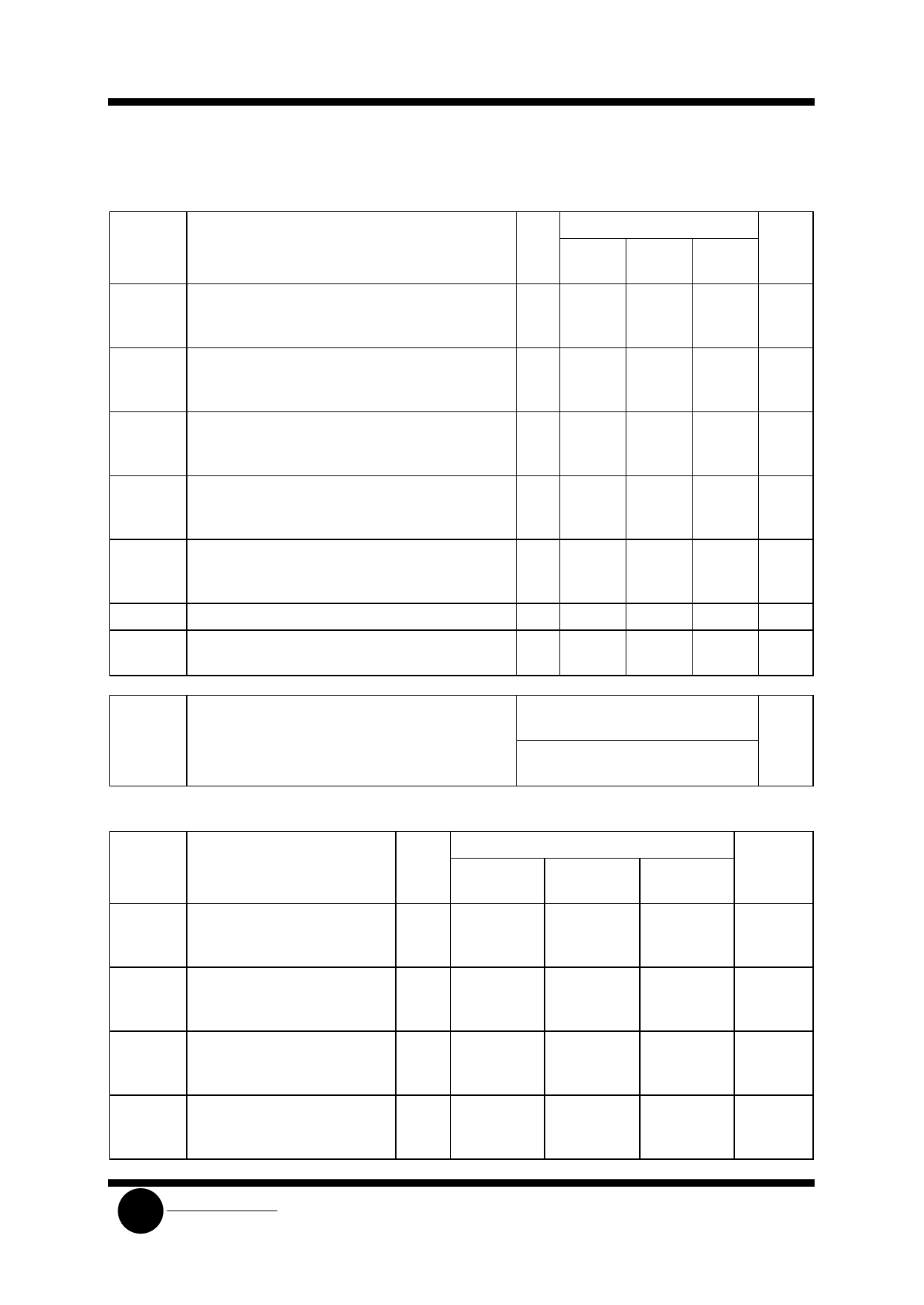
AC ELECTRICAL CHARACTERISTICS(CL=50pF,Input tr=tf=6.0 ns)
Symbol
Parameter
VCC
Guaranteed Limit
V 25 °C to ≤85°C ≤125°C Unit
-55°C
tPLH, tPHL Maximum Propagation Delay, Input D to Q
(Figures 1 and 5)
2.0 125
155
190
ns
4.5 25
31
38
6.0 21
26
32
tPLH, tPHL Maximum Propagation Delay , Latch Enable to Q 2.0 140
175
210
ns
(Figures 2 and 5)
4.5 28
35
42
6.0 24
30
36
tPLZ, tPHZ Maximum Propagation Delay ,Output Enable to Q 2.0 150
190
225
ns
(Figures 3 and 6)
4.5 30
38
45
6.0 26
33
38
tPZL, tPZH Maximum Propagation Delay , Output Enable to Q 2.0 150
190
225
ns
(Figures 3 and 6)
4.5 30
38
45
6.0 26
33
38
tTLH, tTHL Maximum Output Transition Time, Any Output
2.0 60
75
90
ns
(Figures 1 and 5)
4.5 12
15
18
6.0 10
13
15
CIN
Maximum Input Capacitance
COUT Maximum Three-State Output Capacitance
(Output in High-Impedance State)
-
10
10
10
pF
-
15
15
15
pF
Power Dissipation Capacitance (Per Enabled
Output)
CPD Used to determine the no-load dynamic power
consumption: PD=CPDVCC2f+ICCVCC
Typical @25°C,VCC=5.0 V
36
TIMING REQUIREMENTS (CL=50pF,Input tr=tf=6.0 ns)
VCC
Symbol
Parameter
V
tSU
Minimum Setup Time, Input D 2.0
to Latch Enable
4.5
(Figure 4)
6.0
th
Minimum Hold Time,Latch
2.0
Enable to Input D
4.5
(Figure 4)
6.0
tw
Minimum Pulse Width, Latch
2.0
Enable (Figure 2)
4.5
6.0
tr, tf Maximum Input Rise and Fall
2.0
Times (Figure 1)
4.5
6.0
25 °C to
-55°C
25
5.0
5.0
5.0
5.0
5.0
60
12
10
1000
500
400
Guaranteed Limit
≤85°C
30
6.0
6.0
5.0
5.0
5.0
75
15
13
1000
500
400
≤125°C
40
8.0
7.0
5.0
5.0
5.0
90
18
15
1000
500
400
pF
Unit
ns
ns
ns
ns
SLS
System Logic
Semiconductor
Share Link: 