XE9601 Просмотр технического описания (PDF) - Xecom
Номер в каталоге
Компоненты Описание
Список матч
XE9601 Datasheet PDF : 10 Pages
| |||
Pin Descriptions (continued)
PIN NAME I/O
DESCRIPTION
21 GND
— Ground (0 volts)
22 AMP
O Audio output function is set by L & M commands and the value in register S22. This
output can drive a minimum load of 300 ohms.
38 \DCD
O Data Carrier Detect, output, active LO, TTL/CMOS. &C sets the DCD function. In the
default condition, AT&C1, DCD indicates the presense of a carrier signal on the
telephone line.
39 \DSR
O Data Set Ready, output, active LO, TTL/CMOS. &S sets the DSR function. In the default
condition, AT&S0, DSR is forced true.
40 Vcc
— +5 Volts
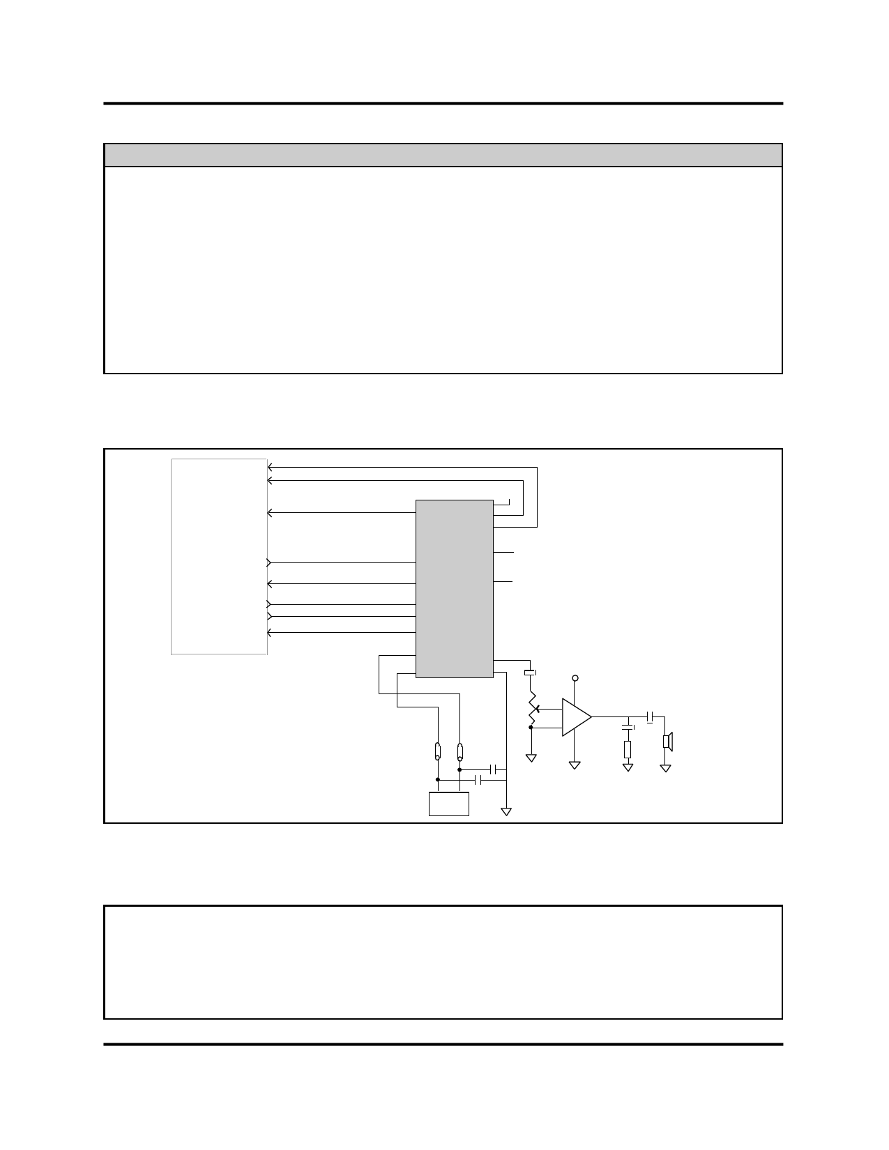
Modem Applications Schematic
/DSR
/DCD
16C450
UART
SIN
VCC
RXD
XE9601
/DSR
/DCD
/DTR
/CTS
SOUT
/RTS
/RI
/DTR
/CTS
TXD
/RTS
/RI
Tip
Ring
Reset
OH
AMP
GND
.2 ufd +5 Volts
50K
L2 L1
C1
LM386
.05 ufd
10 ohms
250 ufd
8 ohm .5 W
Speaker
C2
43
Line
J1
Note: RJ11 Pin assignments reference a 6-pin connector. Tip and Ring are the center pins of all RJ11
jacks.
Recommended Parts
Reference Designation
L1, L2
C1, C2
J1
Description
Ferrite Beads
Capacitors
RJ11 Jack
Recommended Part Number
TDK CB30-1812
Sprague 30GAT47, 470 pfd, 3000 Volts
Stewart SS6446NF
Xecom, Inc.
(3)
XE9601
Share Link: 