SAB-80C535-N Просмотр технического описания (PDF) - Infineon Technologies
Номер в каталоге
Компоненты Описание
Список матч
SAB-80C535-N Datasheet PDF : 56 Pages
| |||
SAB 80C515/80C535
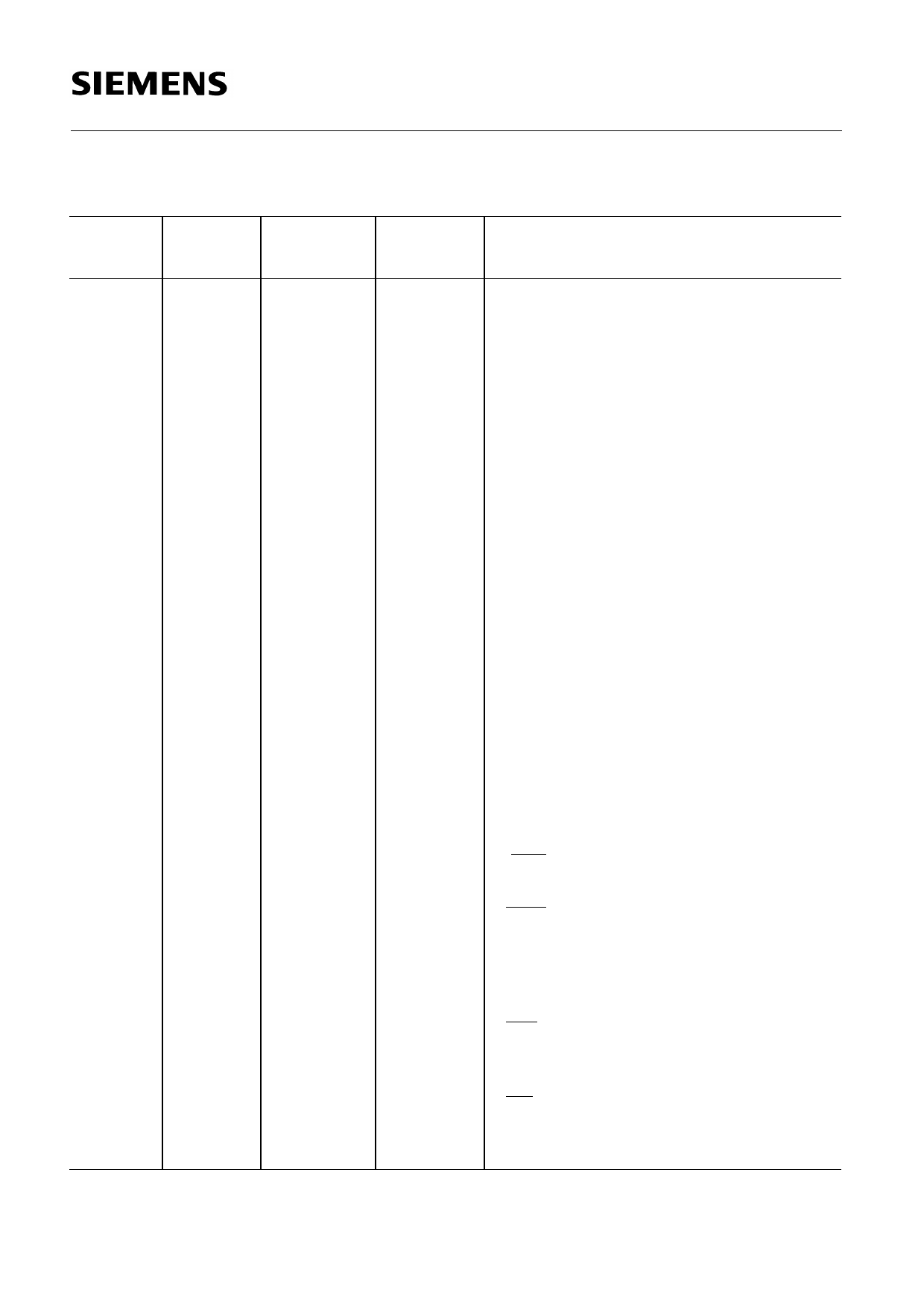
Pin Definitions and Functions (cont’d)
Symbol Pin
Pin
Input (I) Function
P-LCC-68 P-MQFP-80 Output (O)
P3.0-P3.7 21-28
15-22
I/O
Port 3
is an 8-bit bidirectional I/O port with
internal pullup resistors. Port 3 pins that
have1's written to them are pulled high by
the internal pullup resistors, and in that
state can be used as inputs. As inputs,
port 3 pins being externally pulled low will
source current (IIL, in the DC
characteristics) because of the internal
pullup resistors. Port 3 also contains the
interrupt, timer, serial port and external
memory strobe pins that are used by
various options. The output latch
corresponding to a secondary function
must be programmed to a one (1) for that
function to operate. The secondary
functions are assigned to the pins of port
3, as follows:
– R×D (P3.0): serial port's receiver data
input (asynchronous) or data input/
output (synchronous)
– T×D (P3.1): serial port's transmitter data
output
(asynchronous) or clock output
(synchronous)
– INT0 (P3.2): interrupt 0 input/timer 0
gate control input
– INT1 (P3.3): interrupt 1 input/timer 1
gate control input
– T0 (P3.4): counter 0 input
– T1 (P3.5): counter 1 input
– WR (P3.6): the write control signal
latches the data byte from port 0 into the
external data memory
– RD (P3.7): the read control signal
enables the external data memory to
port 0
Semiconductor Group
8
Share Link: 