SAA4951 Просмотр технического описания (PDF) - Philips Electronics
Номер в каталоге
Компоненты Описание
Список матч
SAA4951 Datasheet PDF : 25 Pages
| |||
Philips Semiconductors
Memory controller
Preliminary specification
SAA4951
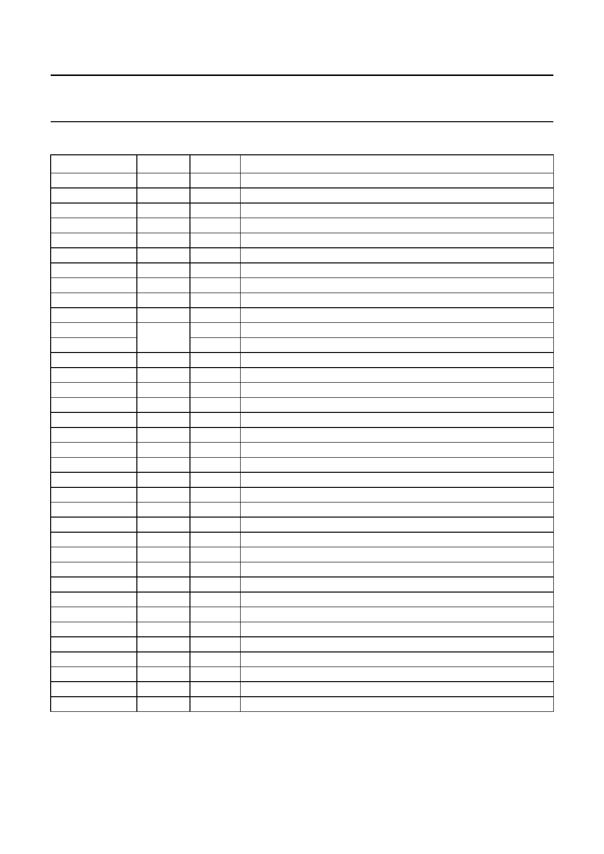
PINNING
SYMBOL
HRD
VDD
SWC1
SRC
SWC2
WEXT
IE1
WE1
STROBE
VDD
HRA
BLNA
VSS
LLA
IE2
WE2
CLV
ALDUV/VB
RE1
RE2
BLND
ALE
WRD
VDD
VSS
P0
P1
P2
P3
P4
P5
P6
P7
LLDFL
VSS
HRDFL
PIN
TYPE(1)
DESCRIPTION
1
O
2
−
horizontal reference signal, display part
positive supply voltage
3
O
serial write clock, memory 1
4
O
serial read clock, memory 1
5
O
serial write clock, memory 2
6
I
external write enable input
7
O
input enable signal, memory 1
8
O
write enable signal, memory 1
9
I
strobe function
10
−
11
O
positive supply voltage
horizontal reference signal, acquisition part
I
horizontal blanking signal, acquisition part
12
−
13
I
ground
line-locked clock signal, acquisition part
14
O
input enable signal, memory 2
15
O
write enable signal, memory 2
16
O
video clamping signal
17
O
acquisition load signal, chrominance U, V / vertical blanking
18
O
read enable signal, memory 1
19
O
read enable signal, memory 2
20
O
horizontal blanking signal, display part
21
I
address latch enable signal
22
I
write/read data signal
23
−
24
−
25
I
positive supply voltage
ground
data input signal, (LSB = least significant bit)
26
I
data input signal
27
I
data input signal
28
I
data input signal
29
I
data input signal
30
I
data input signal
31
I/O
data input/output signal
32
I/O
data input/output signal, (MSB = most significant bit)
33
I
34
−
line-locked clock signal, deflection part
ground
35
O
horizontal reference signal, deflection part
April 1994
4
Share Link: 