RT9701GB Просмотр технического описания (PDF) - Richtek Technology
Номер в каталоге
Компоненты Описание
Список матч
RT9701GB Datasheet PDF : 10 Pages
| |||
RT9701
Thermal Shut
Response
Dowm
CH1
CH3
Thermal Shut Down
CH2
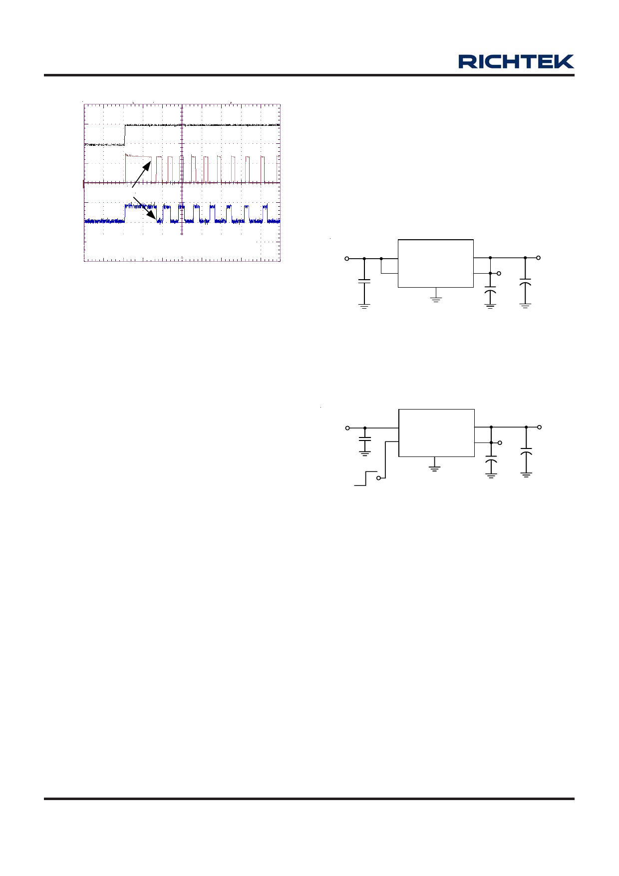
CH1: VEN = 5V/Div, CH3: IOUT@RL1Ω: 1A/Div
CH2: IOUT@short: 1A/DiV, VIN = 5V
Time (50ms/Div)
Application Information
The RT9701 is a high-side single N-Channel MOSFET
switch with active-high enable input.
Input and Output
VIN (input) is the power supply connection to the circuitry
and the drain of the output MOSFET. VOUT (output) is
the source of the output MOSFET. In a typical circuit,
current flows through the switch from VIN to VOUT toward
the load. Both VOUT pins must be short on the board
and connected to the load and so do both VIN pins but
connected to the power source.
Thermal Shutdown
Thermal shutdown shuts off the output MOSFET if the
die temperature exceeds 130°C and 20°C of hysteresis
forces the switch turning off until the die temperature
drops to 110°C.
Soft Start
In order to eliminate the upstream voltage droop caused
by the large inrush current during hot-plug events, the
“soft-start” feature effectively isolates power supplies
from such highly capacitive loads.
Under-voltage Lockout
UVLO prevents the MOSFET switch from turning on until
input voltage exceeds 1.8V (typical). If input voltage drops
below 1.8V (typical), UVLO shuts off the MOSFET switch.
Current Limiting and Short Protection
The current limit circuit is designed to protect the system
supply, the MOSFET switch and the load from damage
caused by excessive currents. The current limit threshold
is set internally to allow a minimum of 1.1A through the
MOSFET but limits the output current to approximately
1.5A typical. When the output is short to ground, it will
limit to a constant current 1A until thermal shutdown or
short condition removed.
VIN
CIN
1uF
RT9701CBL
VIN
VOUT
VIN
VOUT
GND
VOUT1
COUT
VOUT2
COUT
CIN = 1uF, COUT = 470uF (Low ESR) on M/B
CIN = 1uF, COUT = 330uF (Low ESR) on Notebook
CIN = 10uF, COUT = 1uF on USB device
Figure 1. High Side Power Switch
VIN
CIN
Chip Enable
RT9701CB
VIN
VOUT
EN
VOUT
GND
VOUT1
COUT
VOUT2
COUT
Figure 2. High Side Power Switch with Chip Enable
Control
Filtering
To limit the input voltage drop during hot-plug events,
connect a 1μF ceramic capacitor from VIN to GND.
However, higher capacitor values will further reduce the
voltage drop at the input.
Connect a sufficient capacitor from VOUT to GND. This
capacitor helps to prevent inductive parasitics from pulling
VOUT negative during turn-off or EMI damage to other
components during the hot-detachment. It is also
necessary for meeting the USB specification during hot
plug-in operation. If RT9701 is implanted in device end
application, minimum 1μF capacitor from VOUT to GND
is recommended and higher capacitor values are also
preferred.
www.richtek.com
8
DS9701-13 March 2007
Share Link: 