IS61LV2568 Просмотр технического описания (PDF) - Integrated Circuit Solution Inc
Номер в каталоге
Компоненты Описание
Список матч
IS61LV2568 Datasheet PDF : 8 Pages
| |||
IS61LV2568
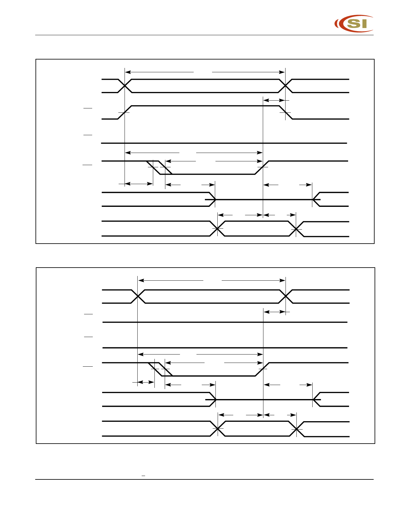
WRITE CYCLE NO. 2(WE Controlled, OE is HIGH During Write Cycle) (1,2)
ADDRESS
OE
t WC
VALID ADDRESS
t HA
CE LOW
WE
DOUT
t SA
DATA UNDEFINED
t AW
t PWE1
t HZWE
DIN
HIGH-Z
t LZWE
t SD
t HD
DATAIN VALID
WRITE CYCLE NO. 3(WE Controlled, OE is LOW During Write Cycle) (1)
ADDRESS
OE LOW
t WC
VALID ADDRESS
t HA
CE LOW
WE
DOUT
t SA
DATA UNDEFINED
DIN
t AW
t PWE2
t HZWE
HIGH-Z
t LZWE
t SD
t HD
DATAIN VALID
Notes:
1. The internal write time is defined by the overlap of CE LOW and WE LOW. All signals must be in valid states to initiate a Write,
but any one can go inactive to terminate the Write. The Data Input Setup and Hold timing are referenced to the rising or falling
edge of the signal that terminates the Write.
2. I/O will assume the High-Z state if OE > VIH.
Integrated Circuit Solution, Inc.
7
SR026-0C
Share Link: 