RT9167 Просмотр технического описания (PDF) - Richtek Technology
Номер в каталоге
Компоненты Описание
Список матч
RT9167 Datasheet PDF : 13 Pages
| |||
RT9167/A
Operating Region and Power Dissipation
The maximum power dissipation of RT9167/A depends
on the thermal resistance of the case and circuit board,
the temperature difference between the die junction and
ambient air, and the rate of airflow. The power dissipation
across the device is P = IOUT (VIN - VOUT). The maximum
power dissipation is: PMAX = (TJ - TA) /θJA
where TJ - TA is the temperature difference between the
RT9167/A die junction and the surrounding environment,
θJA is the thermal resistance from the junction to the
surrounding environment. The GND pin of the RT9167/A
performs the dual function of providing an electrical
connection to ground and channeling heat away. Connect
the GND pin to ground using a large pad or ground plane.
Current Limit and Thermal Protection
T9167 includes a current limit which monitors and controls
the pass transistor's gate voltage limiting the output current
to 350mA Typ. (700mA Typ. for RT9167A). Thermal-
overload protection limits total power dissipation in the
RT9167/A. When the junction temperature exceeds
TJ = +155°C, the thermal sensor signals the shutdown
logic turning off the pass transistor and allowing the IC to
cool. The thermal sensor will turn the pass transistor on
again after the IC's junction temperature cools by 10°C,
resulting in a pulsed output during continuous thermal-
overload conditions. Thermal-overloaded protection is
designed to protect the RT9167/A in the event of fault
conditions. Do not exceed the absolute maximum junction-
temperature rating of TJ = +150°C for continuous operation.
The output can be shorted to ground for an indefinite
amount of time without damaging the part by cooperation
of current limit and thermal protection.
Thermal Considerations
Thermal protection limits power dissipation in RT9167/A.
When the operation junction temperature exceeds 165°C,
the OTP circuit starts the thermal shutdown function and
turns the pass element off. The pass element turn on again
after the junction temperature cools by 30°C.
For continuous operation, do not exceed absolute
maximum operation junction temperature 125°C. The
power dissipation definition in device is:
PD = (VIN − VOUT) x IOUT + VIN x IQ
www.richtek.com
10
The maximum power dissipation depends on the thermal
resistance of IC package, PCB layout, the rate of
surroundings airflow and temperature difference
between junction to ambient. The maximum power
dissipation can be calculated by following formula :
PD(MAX) = ( TJ(MAX) - TA ) / θJA
Where TJ(MAX) is the maximum operation junction
temperature 125°C, TA is the ambient temperature and
the θJA is the junction to ambient thermal resistance.
For recommended operating conditions specification of
RT9167/A, where TJ(MAX) is the maximum junction
temperature of the die (125°C) and TA is the operated
ambient temperature. The junction to ambient thermal
resistance θJA is layout dependent. For SOT-23-5 package,
the thermal resistance θJA is 250°C/W on the standard
JEDEC 51-3 single-layer thermal test board. The maximum
power dissipation at TA = 25°C can be calculated by
following formula :
PD(MAX) = (125°C − 25°C) / 250 = 0.4W for SOT-23-5
package
PD(MAX) = (125°C - 25°C) / 160 = 0.625W for SOP-8
package
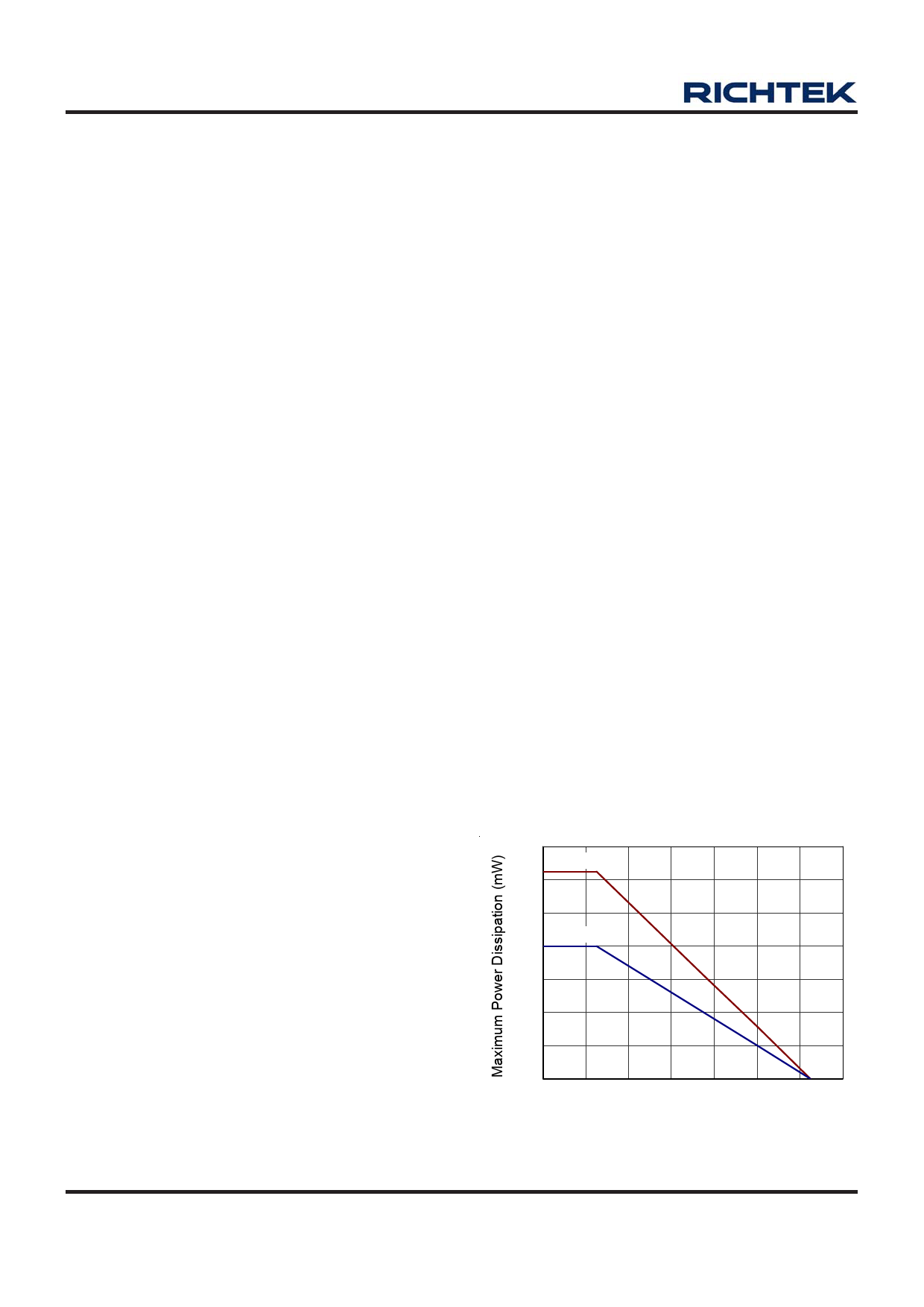
The maximum power dissipation depends on operating
ambient temperature for fixed TJ(MAX) and thermal
resistance θJA. For RT9167/A packages, the Figure 5 of
derating curves allows the designer to see the effect of
rising ambient temperature on the maximum power
allowed.
700
SOP-8
600
500
SOT-23-5
400
300
200
100
0
0
20 40 60 80 100 120 140
Ambient Temperature
Figure 5. Derating Curves for RT9167/A Packages
DS9167/A-26 March 2007
Share Link: 