HM62G36256BP-5 Просмотр технического описания (PDF) - Hitachi -> Renesas Electronics
Номер в каталоге
Компоненты Описание
Список матч
HM62G36256BP-5 Datasheet PDF : 24 Pages
| |||
HM62G36256 Series
Absolute Maximum Ratings
Parameter
Symbol
Value
Unit
Notes
Input voltage on any pin
Core supply voltage
Output supply voltage
Operating temperature
Storage temperature
Junction temperature
VIN
VDD
VDDQ
TOPR
TSTG
Tj
–0.5 to VDDQ + 0.5
V
1, 4
–0.5 to 3.9
V
1
–0.5 to 2.2
V
1, 4
0 to 70
°C
–55 to 125
°C
110
°C
Output short–circuit current
I OUT
25
Latch up current
I LI
200
Package junction to case thermal resistance θJC
5
mA
mA
°C/W 5, 7
Package junction to ball thermal resistance θJB
8
°C/W 6, 7
Notes: 1. All voltage is referred to VSS.
2. Permanent device damage may occur if Absolute Maximum Ratings are exceeded. Functional
operation should be restricted the Operation Conditions. Exposure to higher than recommended
voltages for extended periods of time could affect device reliability.
3. These CMOS memory circuits have been designed to meet the DC and AC specifications shown
in the tables after thermal equilibrium has been established.
4. The supply voltage application sequence need to be powered up in the following manner: VSS,
VDD, VDDQ, VREF then VIN. Remember, according to the Absolute Maximum Ratings table, VDDQ is
not to exceed 3.9 V, whatever the instantaneous value of VDDQ.
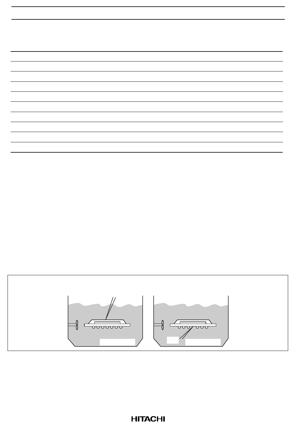
5. θJC is measured at the center of mold surface in fluorocarbon (See Figure “Definition of
Measurement”).
6. θJB is measured on the center ball pad after removing the ball in fluorocarbon (See Figure
“Definition of Measurement”).
7. These thermal resistance values have error of ± 5°C/W.
θJC
θJB
T.C.
Fluorocarbon
T.C. Fluorocarbon
Definition of Measurement
6
Share Link: 