RT8101 Просмотр технического описания (PDF) - Richtek Technology
Номер в каталоге
Компоненты Описание
Список матч
RT8101 Datasheet PDF : 15 Pages
| |||
RT8101/A
Preliminary
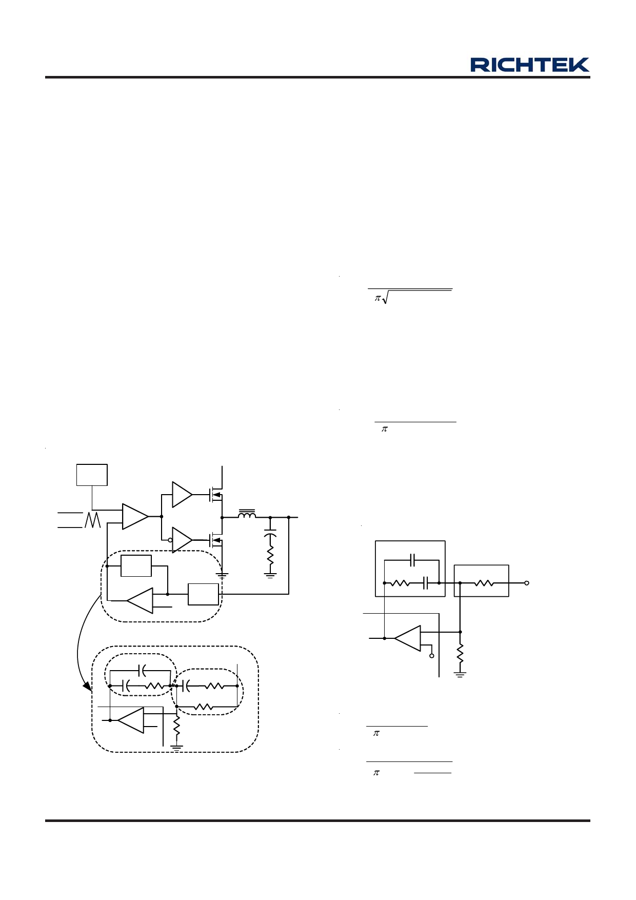
Feedback Compensation
The RT8101/A is a voltage mode controller. The control
loop is a single voltage feedback path including a
compensator and modulator as shown in Figure 5. The
modulator consists of the PWM comparator and power
stage. The PWM comparator compares error amplifier EA
output (COMP) with oscillator (OSC) sawtooth wave to
provide a pulse-width modulated (PWM) with an amplitude
of VIN at the PHASE node. The PWM wave is smoothed
by the output filter LOUT and COUT. The output voltage (VOUT)
is sensed and fed to the inverting input of the error amplifier.
A well-designed compensator regulates the output voltage
to the reference voltage VREF with fast transient response
and good stability.
In order to achieve fast transient response and accurate
output regulation, an adequate compensator design is
necessary. The goal of the compensation network is to
provide adequate phase margin (greater than 45 degrees)
and the highest 0dB crossing frequency. It is also
recommended to manipulate loop frequency response that
its gain crosses over 0dB at a slope of −20dB/dec.
OSC
PWM
Comparator
-
ΔVOSC
+
VIN
Driver
Driver
LOUT
PHASE
COUT
VOUT
ZFB
COMP
-
EA+
ZIN
REF
ESR
C2
ZFB
C1 R2 C3
ZIN VOUT
R3
COMP
R1
-
FB
EA+
REF
Figure 5. Closed Loop
1) Modulator Frequency Equations
The modulator transfer function is the small-signal transfer
function of VOUT/VCOMP (output voltage over the error
amplifier output. This transfer function is dominated by a
DC gain, a double pole, and a zero as shown in Figure 7.
The DC gain of the modulator is the input voltage (VIN)
divided by the peak to peak oscillator voltage VOSC. The
output LC filter introduces a double pole, 40dB/decade
gain slope above its corner resonant frequency, and a total
phase lag of 180 degrees. The resonant frequency of the
LC filter is expressed as below:
fLC =
1
2π LOUT × COUT
The ESR zero is contributed by the ESR associated with
the output capacitance. Note that this requires that the
output capacitor should have enough ESR to satisfy
stability requirements. The ESR zero of the output
capacitor is expressed as follows :
fESR
=
2π
1
× COUT
× ESR
2) Compensation Frequency Equations
The compensation network consists of the error amplifier
and the impedance networks ZC and ZF as shown in
Figure 6.
ZF
C1
R2 C2
ZC
R1
VOUT
- FB
EA
COMP +
VREF
RF
Figure 6. Compensation Loop
fZ1
=
2π
1
x R2 x C2
fP1
=
2π
1
x
R2
x
C1 x
C1 +
C2
C2
www.richtek.com
10
DS8101/A-01 March 2007
Share Link: 