SMD5962-9232404MYX Просмотр технического описания (PDF) - Simtek Corporation
Номер в каталоге
Компоненты Описание
Список матч
SMD5962-9232404MYX Datasheet PDF : 16 Pages
| |||
STK11C68 (SMD5962–92324)
ABSOLUTE MAXIMUM RATINGSa
Voltage on Input Relative to Ground . . . . . . . . . . . . . .–0.5V to 7.0V
Voltage on Input Relative to VSS . . . . . . . . . . –0.6V to (VCC + 0.5V)
Voltage on DQ0-7 . . . . . . . . . . . . . . . . . . . . . . –0.5V to (VCC + 0.5V)
Temperature under Bias . . . . . . . . . . . . . . . . . . . . . –55°C to 125°C
Storage Temperature . . . . . . . . . . . . . . . . . . . . . . . –65°C to 150°C
Power Dissipation . . . . . . . . . . . . . . . . . . . . . . . . . . . . . . . . . . . . 1W
DC Output Current (1 output at a time, 1s duration) . . . . . . . . 15mA
Note a:
Stresses greater than those listed under “Absolute Maximum
Ratings” may cause permanent damage to the device. This is a
stress rating only, and functional operation of the device at condi-
tions above those indicated in the operational sections of this
specification is not implied. Exposure to absolute maximum rat-
ing conditions for extended periods may affect reliability.
DC CHARACTERISTICS
(VCC = 5.0V ± 10%)
SYMBOL
PARAMETER
ICC1b
Average VCC Current
ICC2c
ICC3b
ISB1d
Average VCC Current during STORE
Average VCC Current at tAVAV = 200ns
5V, 25°C, Typical
Average VCC Current
(Standby, Cycling TTL Input Levels)
ISB2d
IILK
IOLK
VIH
VIL
VOH
VOL
TA
VCC Standby Current
(Standby, Stable CMOS Input Levels)
Input Leakage Current
Off-State Output Leakage Current
Input Logic “1” Voltage
Input Logic “0” Voltage
Output Logic “1” Voltage
Output Logic “0” Voltage
Operating Temperature
COMMERCIAL
MIN
MAX
90
75
65
N/A
3
10
27
23
20
N/A
750
INDUSTRIAL/
MILITARY
MIN MAX
90
75
65
55
3
UNITS
mA
mA
mA
mA
mA
10
mA
28
mA
24
mA
21
mA
20
mA
1500 μA
±1
±1
μA
±5
±5
μA
2.2
VSS – .5
2.4
0
VCC + .5
0.8
0.4
70
2.2
VCC + .5 V
VSS – .5 0.8
V
2.4
V
0.4
V
– 40
85
°C
NOTES
tAVAV = 25ns
tAVAV = 35ns
tAVAV = 45ns
tAVAV = 55ns
All Inputs Don’t Care, VCC = max
W ≥ (V CC– 0.2V)
All Others Cycling, CMOS Levels
tAVAV = 25ns, E ≥ VIH
tAVAV = 35ns, E ≥ VIH
tAVAV = 45ns, E ≥ VIH
tAVAV = 55ns, E ≥ VIH
E ≥ (V CC - 0.2V)
All Others VIN ≤ 0.2V or ≥ (VCC – 0.2V)
VCC = max
VIN = VSS to VCC
VCC = max
VIN = VSS to VCC, E or G ≥ VIH
All Inputs
All Inputs
IOUT = – 4mA
IOUT = 8mA
Note b: ICC1 and ICC3 are dependent on output loading and cycle rate. The specified values are obtained with outputs unloaded.
Note c:
Note d:
EICC≥2VisIHthweillanvoetrapgroedcuucreresntat nredqbuyirceudrrfeonr tthleevdeulsrautniotinl
of the STORE cycle (tSTORE ) .
any nonvolatile cycle in progress
has
timed
out.
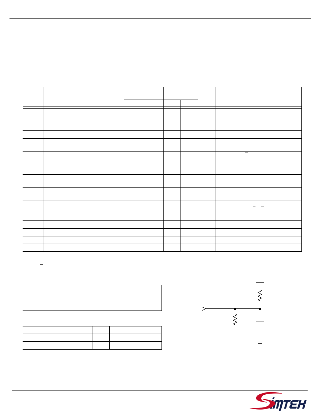
AC TEST CONDITIONS
5.0V
Input Pulse Levels . . . . . . . . . . . . . . . . . . . . . . . . . . . . . . . 0V to 3V
Input Rise and Fall Times . . . . . . . . . . . . . . . . . . . . . . . . . . . . . . . ≤ 5ns
Input and Output Timing Reference Levels . . . . . . . . . . . . . . . 1.5V
Output Load . . . . . . . . . . . . . . . . . . . . . . . . . . . . . . . . . See Figure 1
CAPACITANCEe (TA = 25°C, f = 1.0MHz)
SYMBOL
PARAMETER
MAX UNITS CONDITIONS
CIN
COUT
Input capacitance
8
Output Capacitance 7
pF
ΔV = 0 to 3V
pF
ΔV = 0 to 3V
Note e: These parameters are guaranteed but not tested.
OUTPUT
255 Ohms
480 Ohms
30 pF
INCLUDING
SCOPE AND
FIXTURE
Figure 1: AC Output Loading
Document Control #ML0007 Rev 0.3
3
February, 2007
Share Link: 