RS5C372B-E1 Просмотр технического описания (PDF) - RICOH Co.,Ltd.
Номер в каталоге
Компоненты Описание
Список матч
RS5C372B-E1 Datasheet PDF : 39 Pages
| |||
RS5C372B
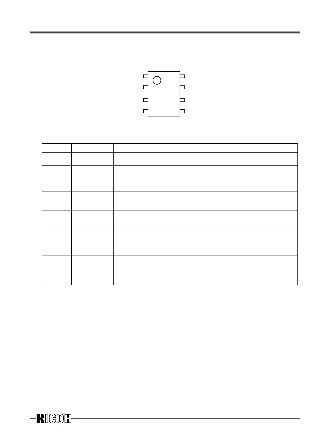
s Pin Configuration
s Pin Description
RS5C372B (8PIN SSOP)
32KOUT 1
SCL 2
8 VDD
7 OSCIN
SDA 3
VSS 4
6 OSCOUT
5 /INTR
TOP VIEW
Symbol
SCL
SDA
Pin Name
Shift clock input
Serial input
output
Description
This pin is used to input shift clock pulses to synchronize data input/output to
and from the SDA pin with this clock. Up to 6V beyond VDD may be input.
This pin inputs and outputs written or read data in synchronization with shift
clock pulses from the SCL pin. Up to 6V beyond VDD may be input. This
pin functions as an Nch open drain output.
/INTR
Interrupt
output
32KOUT 32K Clock
Output
OSCIN Oscillator
OSCOUT circuit
input/output
This pin outputs periodic interrupt pulses and alarm interrupt (ALARM_A,
ALARM_B) to the CPU. This pin is off when power is activated from 0V.
This pin functions as an Nch open drain output.
This pin outputs 32.768kHz pulses (when 32.768kHz crystal is used),
It outputs 32.768kHz when power source is activated from 0V. This pin
functions as an CMOS push-pull output.
These pins configure an oscillator circuit by connecting a 32.768kHz or
32.000kHz crystal oscillator between the OSCIN–OSCOUT pins.
(Any other oscillator circuit components are built into the RS5C372B.)
VDD
VSS
Positive power
supply input
Negative power
supply input
The VDD pin is connected to the positive power supply and Vss to the
ground.
-2-
Share Link: 