RF2958 Просмотр технического описания (PDF) - RF Micro Devices
Номер в каталоге
Компоненты Описание
Список матч
RF2958 Datasheet PDF : 20 Pages
| |||
RF2958
SERIAL DATA INTERFACE
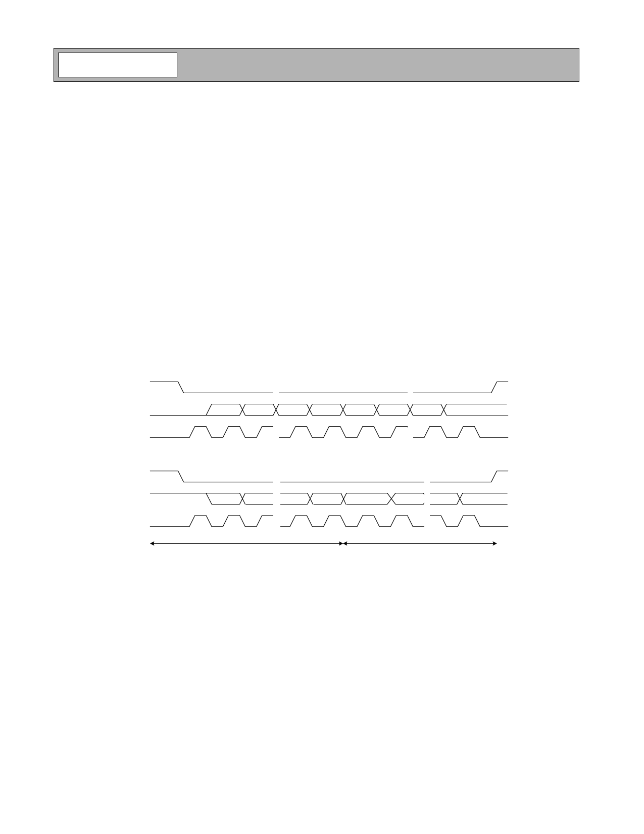
A three wire serial data interface allows user programming of the internal control registers in the RF2958. The serial data
interface consists of the serial select (SSB), serial data in (SDI) and serial clock (SCLK) pins. The SDI is a bi-directional
pin, by default it is configured as an input to the serial interface, but during a read session it is used as an output.
The first bit in a serial transfer (the MSB) is the read/write (R/W) bit. R/W = 1 for a read, and R/W = 0 for a write.
The figure below shows a timing diagram for a serial transfer to the RF2958 serial data interface. The serial select (SSB)
pin is normally high. A serial transfer is initiated by taking SSB low. The address and data bits on the serial data in (SDI)
pin are shifted in on rising edges of the serial clock (SCLK) pin, MSB first. The data is latched and changes take effect on
the falling edge of the clock pulse corresponding to the last (18th) data bit in the addressed register. If the transfer is inter-
rupted, such that the 18th data bit clock pulse does not occur, then no data is written to the register.
When the synthesizers are programmed, an internal pulse is generated alerting the synthesizer that a new setting is
required. In order to guarantee that this internal pulse is long enough, the time between the falling edge of the last serial
clock pulse and the rising edge of SSB must be at least 1/fr.
The RF2958 can be reset to its power on condition (including register defaults) by writing ‘011111b’ plus 18 don’t care
bits to the serial data interface. The reset is actually performed when the SSB is raised after the write. Although this com-
mand can be performed during any settings of the MODE0 and MODE1 pins, care should be taken to ensure that the
registers are reprogrammed in a sufficient time to perform any transmit or receive operations.
Serial Write
SSB
SDI
rw=0
addr4
addr3
addr1
addr0
data17
data16
data1
data0
SCLK
Serial Read
SSB
SDI
rw=1
addr4
addr3
addr1
addr0
data17
data16
data1
data0
SCLK
sdi pin direction - input
sdi pin direction - output
11-274
Rev A0 050209
Share Link: 