RF2942 Просмотр технического описания (PDF) - RF Micro Devices
Номер в каталоге
Компоненты Описание
Список матч
RF2942 Datasheet PDF : 12 Pages
| |||
RF2942
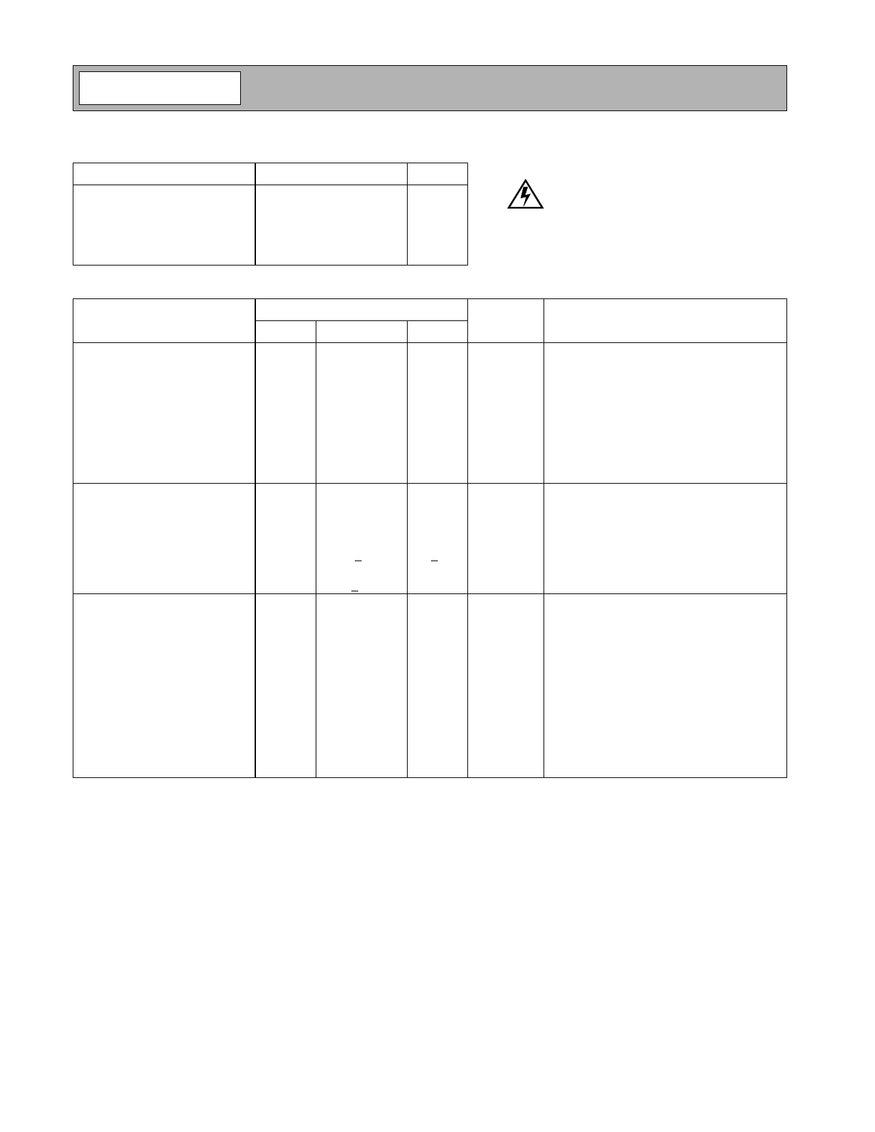
Absolute Maximum Ratings
Parameter
Supply Voltage
Power Down Voltage (VPD)
Input LO and RF Levels
Operating Ambient Temperature
Storage Temperature
Rating
-0.5 to +3.6
VCC + 0.4
+6
-40 to +85
-40 to +150
Unit
VDC
VDC
dBm
°C
°C
Caution! ESD sensitive device.
RF Micro Devices believes the furnished information is correct and accurate
at the time of this printing. However, RF Micro Devices reserves the right to
make changes to its products without notice. RF Micro Devices does not
assume responsibility for the use of the described product(s).
Parameter
Power Supply
Voltage
Current
Carrier Input (LO IN)
Frequency Range
Power Level
Input Impedance
Modulation Input
Frequency Range
Modulation for POUT
Power (I & Q)
Quadrature Phase Error
I/Q Amplitude Imbalance
Input Impedance
RF Output
Power Output
Second Harmonic Output
Third Harmonic Output
Sideband Suppression
Carrier Suppression
Broadband Noise Floor
Specification
Min.
Typ.
Max.
2.8
2.0
3.6
170
225
260
10
24
1800 to 1860
-15
-6
50
DC
2
10
400
+2
+5
0.2
>10
23
21
22
27
-20
-25
-35
-45
-25
-40
-25
-90
Unit
Condition
V
V
mA
mA
MHz
dBm
Ω
Specifications
Operating limits
TXEN = 0.0 V
T=25 °C, VCC=2.8V
1830 MHz
MHz
mVP-P
°
dB
kΩ
dBm
dBm
dBc
dBc
dBc
dBc
dBm/Hz
50Ω source, I,Q=400mVp-p
Differential
T=25°C, VCC=2.8V, LO power=-6dBm,
SSB, I/Q=400mVP-P sine wave, 500kHz
VCC = 3.0 V
VCC = 2.8 V
Modulation DC offset can be externally
adjusted for optimum suppression. Carrier
suppression is then typically better than
40 dB.
11-196
Rev A4 040115
Share Link: 