RF2938 Просмотр технического описания (PDF) - RF Micro Devices
Номер в каталоге
Компоненты Описание
Список матч
RF2938 Datasheet PDF : 20 Pages
| |||
RF2938
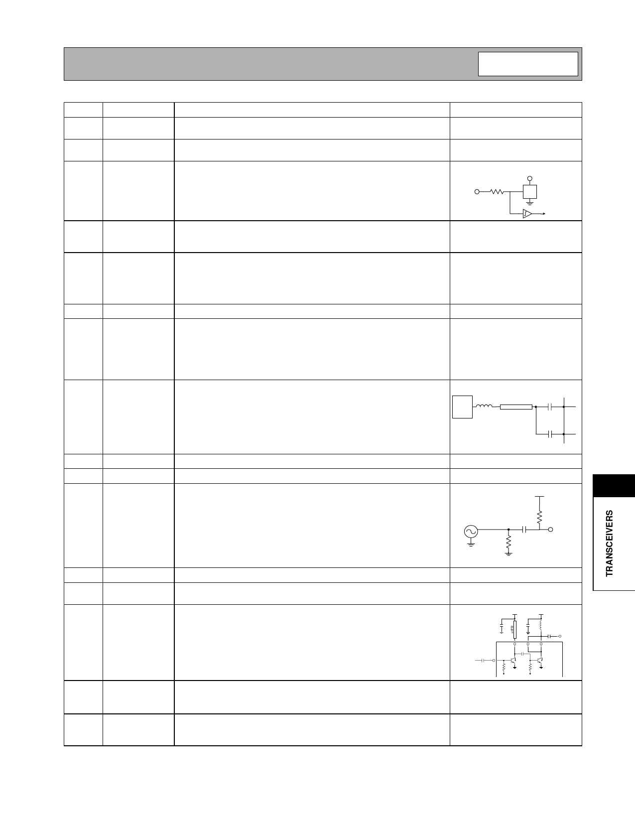
Pin
1
2
3
4
5
6
7
8
9
10
11
12
13
14
15
16
Function
NC
NC
PD
RX EN
TX EN
VCC1
RX IF IN
TX IF IN
VCC9
TX VGC
IF LO
VCC8
NC
RF OUT
RF OUT
VCC6
Description
Interface Schematic
No internal connection. May be grounded or connected on adjacent
signal or left floating. Connect to ground for best results.
No internal connection. May be grounded or connected on adjacent
signal or left floating. Connect to ground for best results.
This pin is used to power up or down the transmit and receive base-
band sections. A logic high powers up the quad demod mixers, TX and
RX GmC LPF’s, baseband VGA amps, data amps, and IF LO buffer
amp/ phase splitter. A logic low powers down the entire IC for sleep
Pins
3, 4, 5
10k Ω
mode. Also, see State Decode Table.
VCC
ESD
To Logic
Enable pin for the receiver 15dB gain IF amp and the RX VGA amp.
Powers up all receiver functions when PD is high, turns off the receiver
IF circuits when low. Also, see State Decode Table.
This pin is used to enable the transmit upconverter, buffer amps, 15db
IF amp, quad mod mixers, TX LO buffer, TX VGA, and PA driver. TX EN
is active low, when TX EN <1V, the transmit circuit is active if PD is
high. A logic high (TX EN >2V) disables the transmit IF/RF circuitry and
quad mod. Also, see State Decode Table.
Power supply for RX VGA amplifier, IC logic and RX references.
See pin 3.
See pin 3.
IF input for receiver section. Must have DC blocking cap. The capacitor
value should be appropriate for the IF frequency. External matching to
50Ω recommended. For half duplex operation, connect RX IF IN and
TX IF IN signals together after the DC blocking caps, then run a trans-
mission line from the output of the IF SAW. AC coupling capacitor must
be less than 150pF to prevent delay in switching RX to TX/TX to RX.
Input for the TX IF signal after SAW filter. External DC blocking cap
required. External matching to 50Ω recommended. For half duplex
operation, connect RX IF IN and TX IF IN signals together after the DC
blocking caps, then run a transmission line from the output of the IF
SAW. AC coupling capacitor must be less than 150pF to prevent delay
in switching RX to TX/TX to RX.
See pin 8.
IF
SAW
Filter
50 Ω µstrip
DC Block Pin 7
Pin 8
Power supply for the TX 15dB gain amp and TX VGA.
Gain control setting for the transmit VGA. Positive slope.
IF LO input. Must have DC blocking cap. The capacitor value should be
appropriate for the IF frequency. LO frequency=2xIF. Quad mod/
demod phase accuracy requires low harmonic content from IF LO, so it
is recommended to use an n=3 LPF between the IF VCO and IF LO.
This is a high impedance input and the recommended matching
approach is to simply add a 100Ω shunt resistor at this input to con-
strain the mismatch. This pin requires a 6.5µA DC bias current. This
can be accomplished with a 270kΩ resistor to VCC for 3.3V operation.
VCC
Recommended Matching
Network for IF LO
IF VCO
C2
150 pF
270 kΩ
IF LO
Pin 11
100 Ω
Power supply for IF LO buffer and quadrature phase network.
No internal connection. May be grounded or connected on adjacent
signal or left floating. Connect to ground for best results.
This is the output transistor of the power amp stage. It is an open col-
lector output. The output match is formed by an inductor to VCC, which
supplies DC and a series cap.
VCC
VCC
CBYP
22 nF
CBYP
22 nF
From
TX RF
Image Filter
PA IN
Pin 18
VCC6
Pin 16
14 mA
PA OUT PA OUT
Pin 14
Pin 15
34 mA
Bias
Bias
Power
Amp
Output
This is the output transistor of the power amp stage. It is an open col-
lector output. The output match is formed by an inductor to VCC, which
supplies DC and a series cap.
Power supply for the PA driver amp. This inductance to ground via
decoupling, along with an internal series capacitor, forms the interstage
match.
See pin 14.
See pin 14.
11
Rev A8 010418
2-5
Share Link: 