R5F21226DFP Просмотр технического описания (PDF) - Renesas Electronics
Номер в каталоге
Компоненты Описание
Список матч
R5F21226DFP Datasheet PDF : 54 Pages
| |||
R8C/22 Group, R8C/23 Group
1. Overview
1.6 Pin Functions
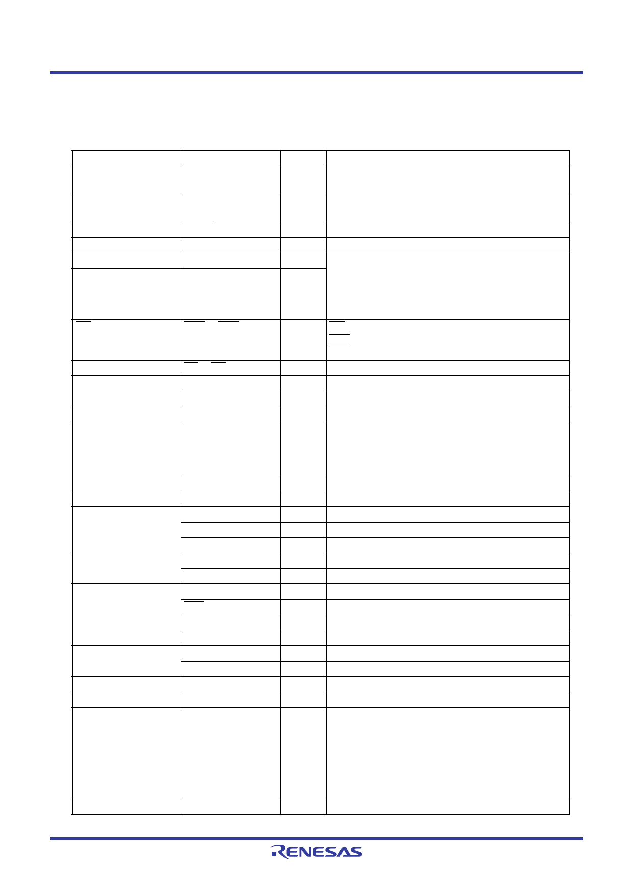
Table 1.5 lists the Pin Functions and Table 1.6 lists the Pin Name Information by Pin Number.
Table 1.5 Pin Functions
Type
Symbol
I/O Type
Description
Power Supply Input
VCC
VSS
I
Apply 2.7 V to 5.5 V to the VCC pin. Apply 0 V to the
VSS pin.
Analog Power Supply AVCC, AVSS
Input
I
Applies the power supply for the A/D converter. Connect
a capacitor between AVCC and AVSS.
Reset Input
RESET
I
Input “L” on this pin resets the MCU.
MODE
MODE
I
Connect this pin to VCC via a resistor.
XIN Clock Input
XIN Clock Output
XIN
XOUT
I
These pins are provided for the XIN clock generation
O circuit I/O. Connect a ceramic resonator or a crystal
oscillator between the XIN and XOUT pins. To use an
externally derived clock, input it to the XIN pin and leave
the XOUT pin open.
INT Interrupt Input
INT0 to INT3
I
INT interrupt input pins.
INT0 Timer RD input pins.
INT1 Timer RA input pins.
Key Input Interrupt
KI0 to KI3
I
Key input interrupt input pins.
Timer RA
TRAIO
I/O Timer RA I/O pin.
TRAO
O Timer RA output pin.
Timer RB
TRBO
O Timer RB output pin.
Timer RD
TRDIOA0, TRDIOA1,
TRDIOB0, TRDIOB1,
TRDIOC0, TRDIOC1,
TRDIOD0, TRDIOD1
I/O Timer RD I/O ports.
TRDCLK
I
External clock input pin.
Timer RE
TREO
O Divided clock output pin.
Serial Interface
CLK0
I/O Transfer clock I/O pin.
RXD0, RXD1
I
Serial data input pins.
TXD0, TXD1
O Serial data output pins.
I2C Bus Interface
SCL
I/O Clock I/O pin.
SDA
I/O Data I/O pin.
Clock Synchronous
Serial I/O with Chip
Select
SSI
SCS
SSCK
I/O Data I/O pin.
I/O Chip-select signal I/O pin.
I/O Clock I/O pin.
SSO
I/O Data I/O pin.
CAN Module
CRX0
I
CAN data input pin.
CTX0
O CAN data output pin.
Reference Voltage Input VREF
I
Reference voltage input pin to A/D converter.
A/D Converter
AN0 to AN11
I
Analog input pins to A/D converter.
I/O Port
P0_0 to P0_7,
P1_0 to P1_7,
P2_0 to P2_7,
P3_0, P3_1,
P3_3 to P3_5, P3_7,
P4_3 to P4_5,
P6_0 to P6_7
I/O CMOS I/O ports. Each port contains an input/output
select direction register, allowing each pin in that port to
be directed for input or output individually.
Any port set to input can select whether to use a pull-up
resistor or not by a program.
Input Port
P4_2, P4_6, P4_7
I
Input only ports.
I: Input O: Output
I/O: Input and output
Rev.2.00 Aug 20, 2008 Page 8 of 48
REJ03B0097-0200
Share Link: 