PMB2341 Просмотр технического описания (PDF) - Infineon Technologies
Номер в каталоге
Компоненты Описание
Список матч
PMB2341 Datasheet PDF : 26 Pages
| |||
Confidential
PMB 2341
preliminary
Functional Description
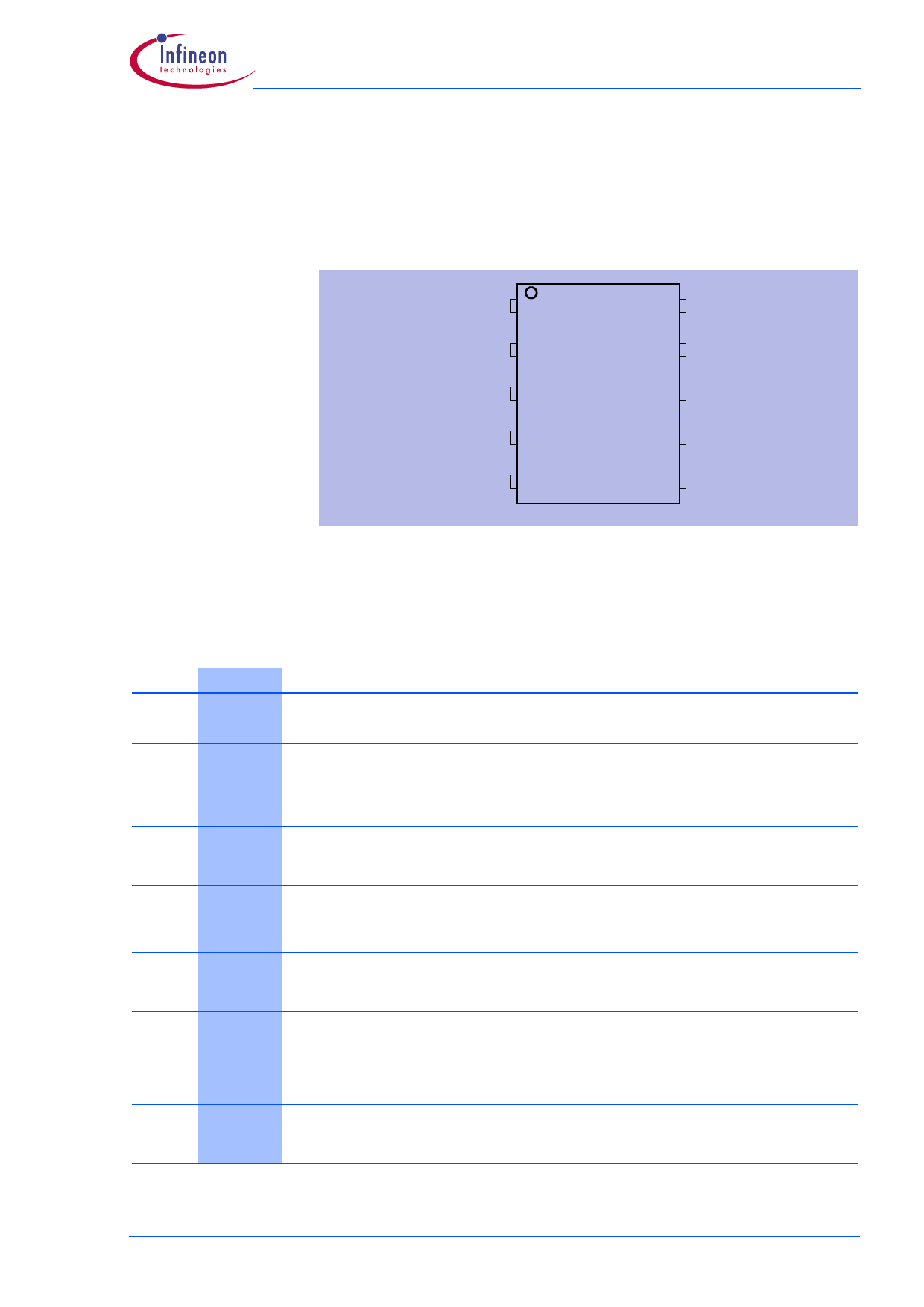
3.1 Pin Configuration
VDD 1
10 RI
CP 2
9 EN
GND 3 PMB 2341 8 DA
LO 4
7 CLK
VCC 5
6 MFO
Figure 3-1 IC Pin Configuration
Pin_config.wmf
3.2 Pin Definition and Functions
Pin No.
1
2
3
Symbol
VDD
CP
GND
4
LO
5
VCC
6
MFO
7
CLK
8
DA
9
EN
10
RI
Function
Digital CMOS supply voltage. Note: VDD and VCC must be equal!
PLL charge pump output
Analog / bipolar ground, Charge pump ground and Digital CMOS ground (VSS)
Used for bipolar prescaler, charge pump and Digital CMOS
RF frequency input
AC coupling is required.
Analog / bipolar supply and Charge pump supply
Used for bipolar prescaler, input buffer and chargepump
Note: VDD and VCC must be equal!
Multi-functional output (Open-drain)
3-Wire bus input: Clock
Clock input of the serial control interface with CMOS Schmitt-Trigger input stage
3-Wire bus input: Data
Data input of the serial control interface withCMOS Schmitt-Trigger input stage.The serial
data are read into the addressed internal shift register with the positive edge of CLK
3-Wire bus input: Enable
Enable input of serial control interface with CMOS Schmitt-Trigger input stage. When
EN=H the input signals CLK and DA are disabled. When EN=L the serial control interface
is enabled. The received data bits are transmitted into the addressed registers with the
positive edge of EN
Reference frequency input
Input with highly sensitive preamplifier. With small input signals AC coupling must be set
up, whereas DC coupling can be used for large input signals
Wireless Components
3-2
Specification, February 2000
Share Link: 