W83194R-81 Просмотр технического описания (PDF) - Winbond
Номер в каталоге
Компоненты Описание
Список матч
W83194R-81 Datasheet PDF : 18 Pages
| |||
W83194R-81
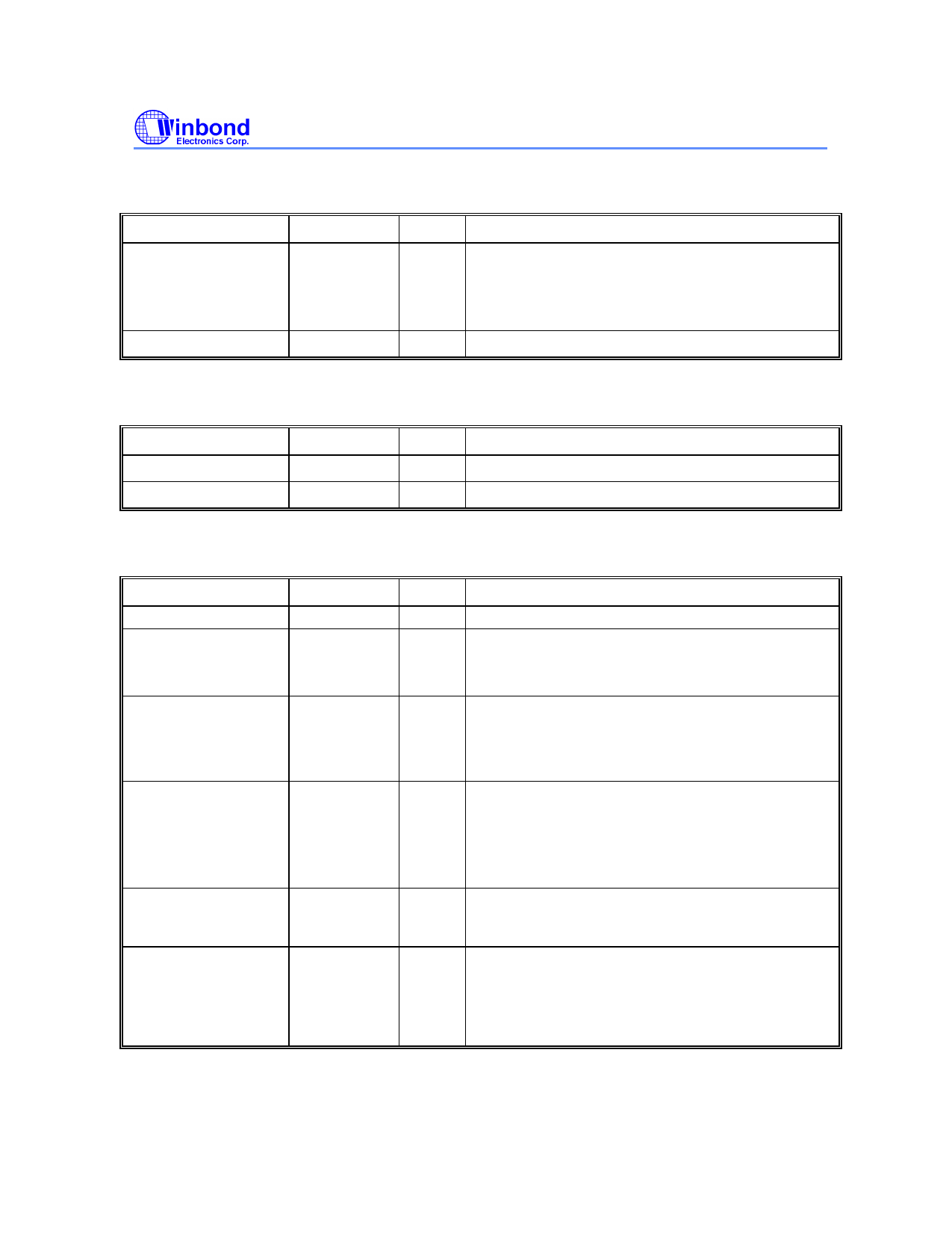
5.2 CPU, SDRAM, PCI Clock Outputs, continued
SYMBOL
PIN
PCICLK 0 / *FS2
8
PCICLK [ 1:4 ]
10,11,12,13
PRELIMINARY
I/O
I/O
OUT
FUNCTION
Latched input for FS2 at initial power up for H/W
selecting the output frequency of CPU, SDRAM and
PCI clocks.
PCI clock during normal operation.
Low skew (< 250ps) PCI clock outputs.
5.3 I2C Control Interface
SYMBOL
PIN
*SDATA
23
*SDCLK
24
I/O
FUNCTION
I/O Serial data of I2C 2-wire control interface
IN Serial clock of I2C 2-wire control interface
5.4 Fixed Frequency Outputs
SYMBOL
PIN
IOAPIC
47
REF0 / *MODE
2
REF1 /*SD_SEL#
46
REF2 / CPU3.3#_2.5
44
SIO / *SEL24_14#
25
48MHz / *FS0
26
I/O
FUNCTION
O 2.5V fixed 14.318MHz
I/O 3.3V, 14.318MHz reference clock output.
Internal 250kΩ pull-up.
Function select pin.
I/O 3.3V, 14.318MHz reference clock output
Internal 250kΩ pull-up.
Latched input at Power On selects the frequencies
for clock outputs.
I/O Internal 250kΩ pull-up.
Latched input for CPU3.3#_2.5 at initial power up.
Reference clock during normal operation.
Latched high - Vddq2b = 2.5V
Latched low - Vddq2b = 3.3V
I/O *SEL24_14# controls the frequency of SIO. If logic 0
at power on, SIO=14.318. If logic 1, SIO=24MHz for
super I/O.
I/O Internal 250kΩ pull-up.
Latched input for FS0 at initial power up for H/W
selecting the output frequency of CPU, SDRAM and
PCI clocks. 48MHz output for USB during normal
operation.
Publication Release Date: Dec. 1998
-4-
Revision 0.20
Share Link: 