W83194R-58 Просмотр технического описания (PDF) - Winbond
Номер в каталоге
Компоненты Описание
Список матч
W83194R-58 Datasheet PDF : 19 Pages
| |||
Preliminary W83194R-37/-58
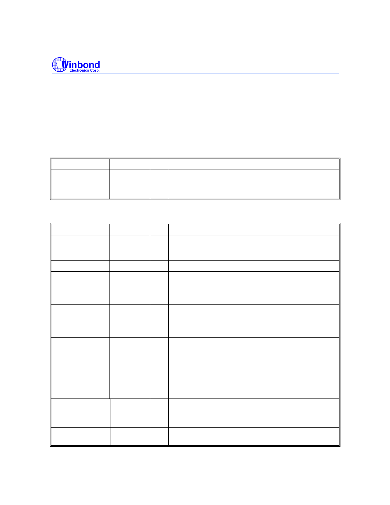
5.0 PIN DESCRIPTION
IN - Input
OUT - Output
I/O - Bi-directional Pin
# - Active Low
* - Internal 250kΩ pull-up
5.1 Crystal I/O
SYMBOL
PIN
Xin
4
Xout
5
I/O
FUNCTION
IN Crystal input with internal loading capacitors and feedback
resistors.
OUT Crystal output at 14.318 MHz nominally.
5.2 CPU, SDRAM, PCI Clock Outputs
SYMBOL
CPUCLK [ 0:3 ]
AGP[ 0:1]
SDRAM11/
CPU_STOP#
SDRAM10/
PCI_STOP#
SDRAM [ 0:9]
PCICLK_F/ *FS1
PCICLK 0/ *FS2
PCICLK [ 1:4 ]
PIN
40, 41, 43,
44
15, 47
17
18
20, 21, 28,
29, 31, 32,
34, 35, 37,
38
7
8
10, 11, 12,
13
I/O
FUNCTION
OUT Low skew (< 250 pS) clock outputs for host frequencies
such as CPU, Chipset and Cache. VDDq2b is the supply
voltage for these outputs.
OUT Accelerate Graphic Port clock outputs
I/O If MODE = 1 (default), then this pin is a SDRAM clock
buffered output of the crystal. If MODE = 0, then this pin is
CPU_STOP# input used in power management mode for
synchronously stopping the all CPU clocks.
I/O If MODE = 1 (default), then this pin is a SDRAM clock
output. If MODE = 0, then this pin is PCI_STOP # and
used in power management mode for synchronously
stopping the all PCI clocks.
O SDRAM clock outputs which have the same frequency as
CPU clocks.
I/O Latched input for FS1 at initial power up for H/W selecting
the output frequency of CPU, SDRAM and PCI clocks.
Free running PCI clock during normal operation.
I/O Latched input for FS2 at initial power up for H/W selecting
the output frequency of CPU, SDRAM and PCI clocks.
PCI clock during normal operation.
OUT Low skew (< 250 pS) PCI clock outputs.
Publication Release Date: April 1999
-3-
Revision A1
Share Link: 