W83194R-17A Просмотр технического описания (PDF) - Winbond
Номер в каталоге
Компоненты Описание
Список матч
W83194R-17A Datasheet PDF : 21 Pages
| |||
W83194R-17/-17A
10.0 POWER MANAGEMENT TIMING
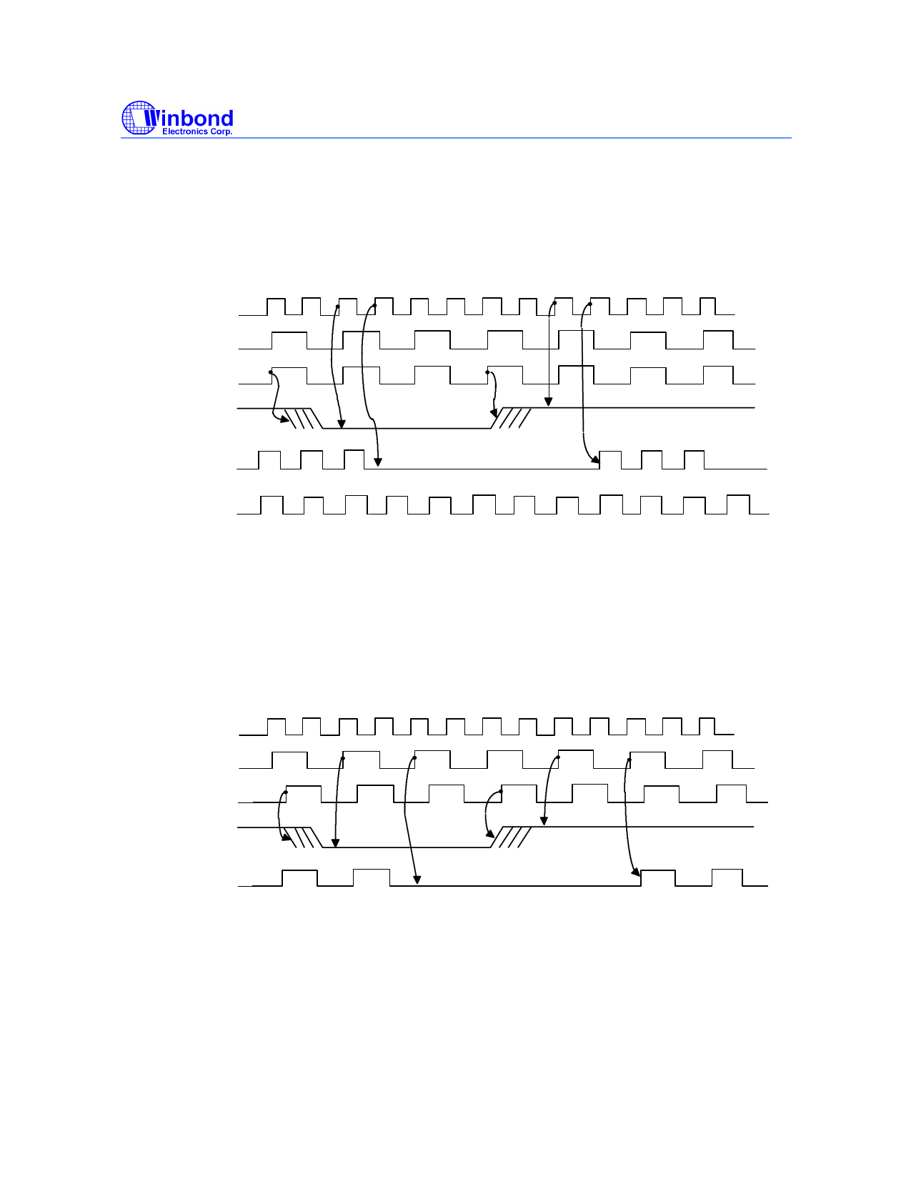
10.1 CPU_STOP# Timing Diagram
PRELIMINARY
CPUCLK
(Internal)
PCICLK
(Internal)
PCICLK_F
CPU_STOP#
CPUCLK[0:3]
1
2
1
2
SDRAM
For synchronous Chipset, CPU_STOP# pin is a synchronous “active low ”input pin used to stop the
CPU clocks for low power operation. This pin is asserted synchronously by the external control logic
at the rising edge of free running PCI clock(PCICLK_F). All other clocks will continue to run while
the CPU clocks are stopped. The CPU clocks will always be stopped in a low state and resume
output with full pulse width. In this case, CPU “clocks on latency“is less than 2 CPU clocks and
“clocks off latency” is less then 2 CPU clocks.
10.2 PCI_STOP# Timing Diagram
CPUCLK
(Internal)
PCICLK
(Internal)
PCICLK_F
PCI_STOP#
1
2
1
2
PCICLK[0:4]
For synchronous Chipset, PCI_STOP# pin is a synchronous “active low”input pin used to stop the
PCICLK [0:4] for low power operation. This pin is asserted synchronously by the external control logic
at the rising edge of free running PCI clock(PCICLK_F). All other clocks will continue to run while
the PCI clocks are stopped. The PCI clocks will always be stopped in a low state and resume output
with full pulse width. In this case, PCI “clocks on latency“is less than 1 PCI clocks and “clocks off
latency” is less then 1 PCI clocks.
- 16 -
Publication Release Date: Sep. 1998
Revision 0.20
Share Link: 