LC86E5032 Просмотр технического описания (PDF) - SANYO -> Panasonic
Номер в каталоге
Компоненты Описание
Список матч
LC86E5032 Datasheet PDF : 21 Pages
| |||
LC86E5032
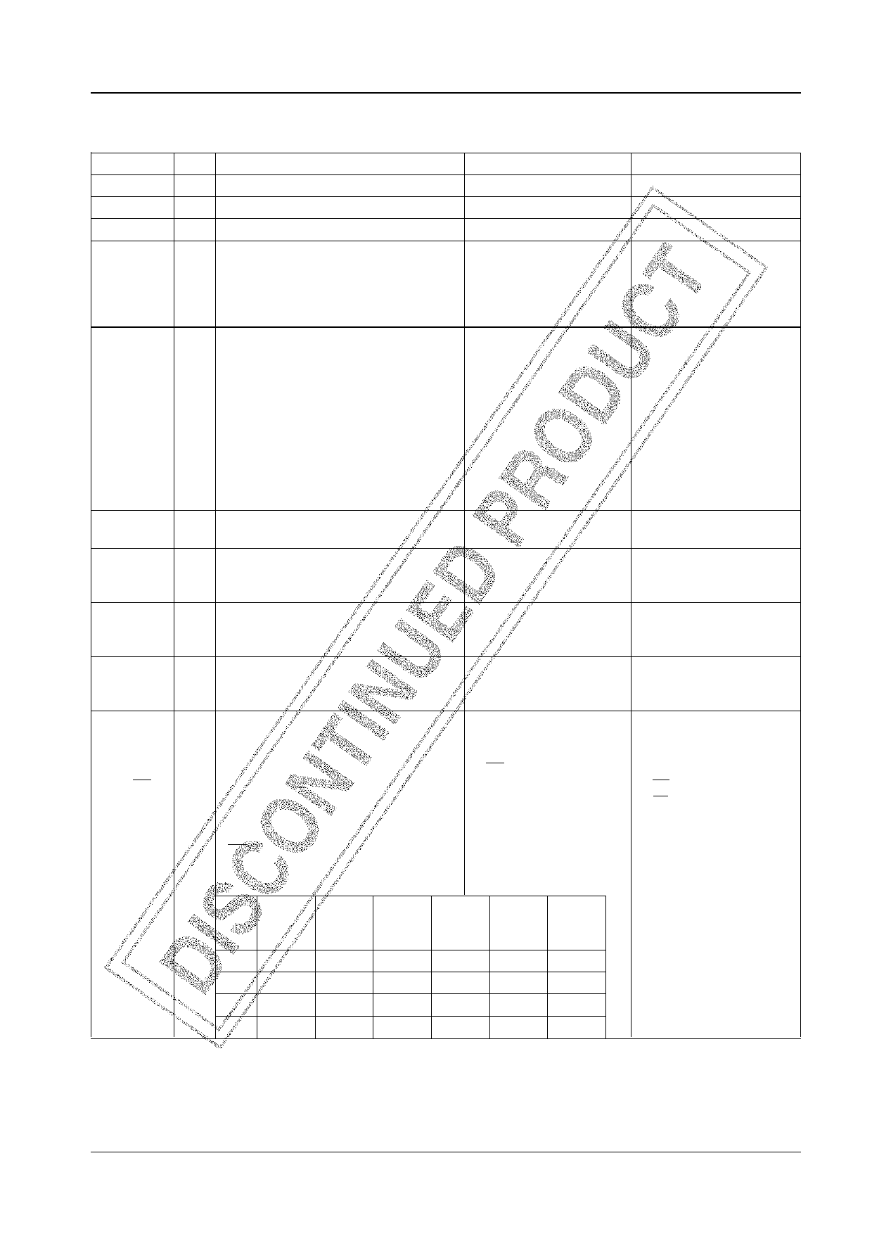
LC86E5032 Pin Description
Pin name
VSS
VDD
VDDVPP
PORT0
P00 to P07
PORT1
P10 to P17
PORT2
P20 to P27
PORT3
P30 to P37
PORT4
P40 to P47
PORT5
P50 to P51
PORT7
P70
P71 to P74
I/O
Function description
Option
Power supply pin (–)
Power supply pin (+)
Power supply pin (+)
I/O • 8-bit input/output port
• Input for port 0 interrupt
• Input/output in nibble units
• Input for HOLD release
• Pull-up resistor :
Present/Not present
• Output form : CMOS/
N-channel open-drain.
I/O • 8-bit input/output port
Output form : CMOS/
• Data direction can be specified for each bit. N-channel open-drain
• Other pin functions
P10 : SIO0 data output
P11 : SIO0 data input/bus input/output
P12 : SIO0 clock input/output
P13 : SIO1 data output
P14 : SIO1 data input/ bus input/output
P15 : SIO1 clock input/output
P16 : Buzzer output
P17 : Timer 1 output (PWM output)
I/O • 8-bit input/output port
Output form : CMOS/
• Data direction can be specified for each bit. N-channel open-drain
I/O • 8-bit input/output port
Output form : CMOS/
• Data direction can be specified for each bit. N-channel open-drain
• 15 V withstand at N-ch open-drain output
I/O • 8-bit input/output port
Output form : CMOS/
• Data direction can be specified for each bit. N-channel open-drain
• 15 V withstand at N-ch open-drain output
I/O • 2-bit input/output port.
Output form : CMOS/
• Data direction can be specified for each bit. N-channel open-drain
• 15 V withstand at N-ch open-drain output
• 5-bit input port
Pull-up resistor :
• Other pin functions
Present/Not present
I/O P70 : INT0 input/HOLD release/N-channel (P70, 71, 72, 73)
transistor output for watchdog timer. * P74 has no pull-up
I
P71 : INT 1 input/HOLD release.
resistor.
P72 : INT 2 input/timer 0 event input.
P73 : INT 3 input with noise filter/timer 0
event input.
P74 : Input pin XT1 for 32.768 kHz crystal
oscillation
• Interrupt received format, vector address.
Rising
Falling
Rising
&
falling
High
level
Low
level
Vector
INT0 Enable Enable Disable Enable Enable 03H
INT1 Enable Enable Disable Enable Enable 0BH
INT2 Enable Enable Enable Disable Disable 13H
INT3 Enable Enable Enable Disable Disable 1BH
Function in PROM mode
Power for programming
Data input/output
• D0 to D7
Address input
• A7 to A0
Address input
• A14 to A8 (*5)
• P47 : TA (*4)
Input of PROM control signal
• DASEC (*1)
• OE (*2)
• CE (*3)
No. 5632-8/21
Share Link: 