PI74ALVCH16344 Просмотр технического описания (PDF) - Pericom Semiconductor
Номер в каталоге
Компоненты Описание
Список матч
PI74ALVCH16344 Datasheet PDF : 7 Pages
| |||
PI74ALVCH16344
123456789012345678901234567890121234567890123456789012345678901212345678910-1B23i4t56t7o89401-2B34i5t6A789d0d12r1e23s4s56D78r90iv12e3r45w678i9t0h12334-5S67t8a90t1e21O23u45t6p78u9t01s2
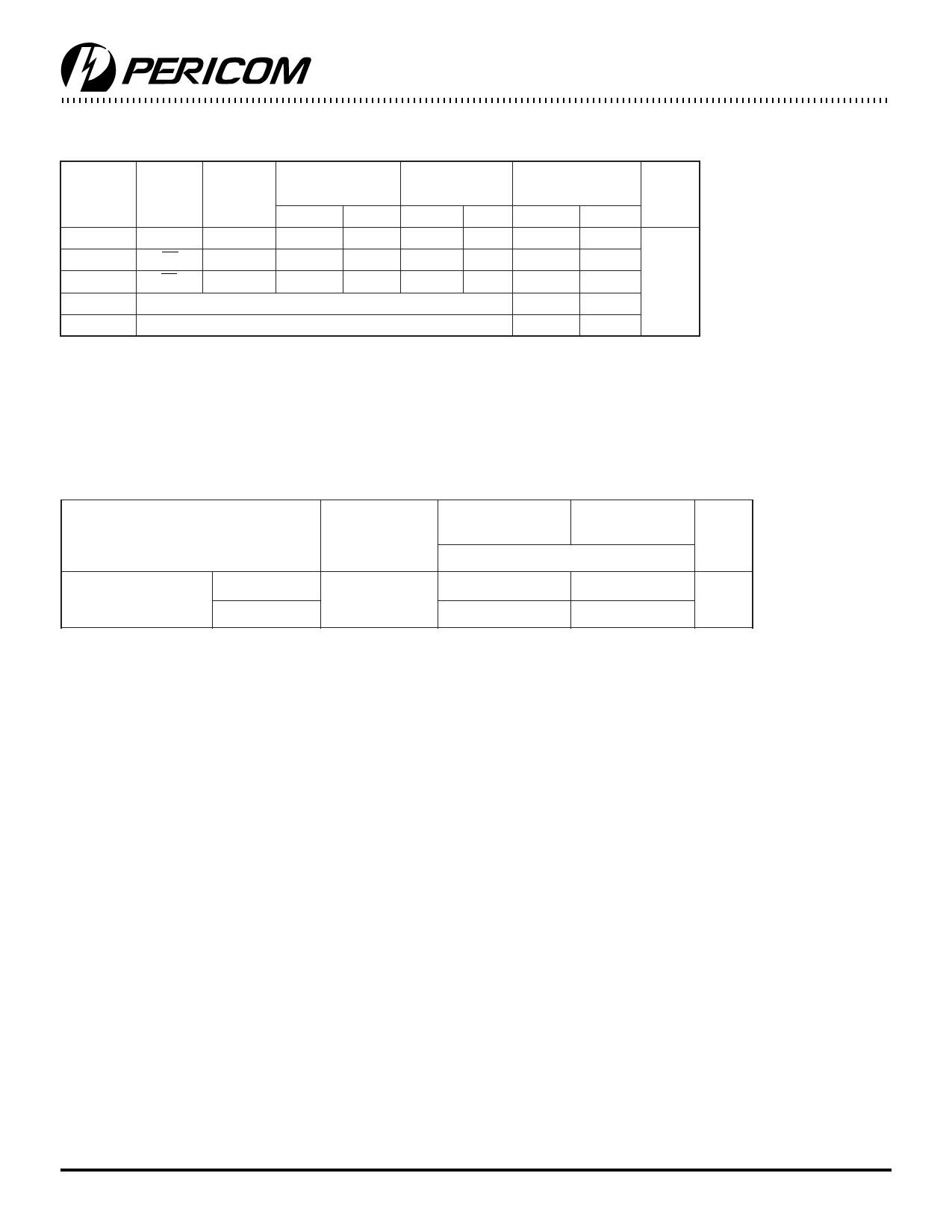
Switching Characteristics over Operating Range(1)
Parameters
From
(INPUT)
To VCC = 2.5V ± 0.2V
(OUTPUT) Min.(2) Max.
VCC = 2.7V VCC = 3.3V ± 0.3V
Min.(2) Max. Min.(2) Max.
tPD
A
B
1.0
5.0
tEN
OE
B
1.0
6.8
tDIS
OE
B
1.0
6.0
tsk(0)(3)
tsk(0)(4)
4.0
1.0
3.6
6.0
1.0
5.0
5.2
1.0
5.0
-
0.35
-
0.5
Notes:
1. See test circuit and waveforms, Figures 1 and 2.
2. Minimum limits are guaranteed but not tested on Propagation Delays.
3. Skew between outputs of same bank, and same device and same transition.
This parameter is warranted but not production tested.
4. Skew between outputs of all banks, and same device, A1-A8 tied together.
This parameter is warranted but not production tested.
Units
ns
Operating Characteristics, TA = 25ºC
Parameter
Test Conditions
CPD Power Dissipation Outputs Enabled
Capacitance
Outputs Disabled
CL = 50pF,
f = 10 MHz
VCC = 2.5V
± 0.2V
VCC = 3.3V ±
0.3V
Typical
68
84
11
14
Units
pF
5
PS8166B 10/19/99
Share Link: 