74ACT818 Просмотр технического описания (PDF) - Fairchild Semiconductor
Номер в каталоге
Компоненты Описание
Список матч
74ACT818 Datasheet PDF : 6 Pages
| |||
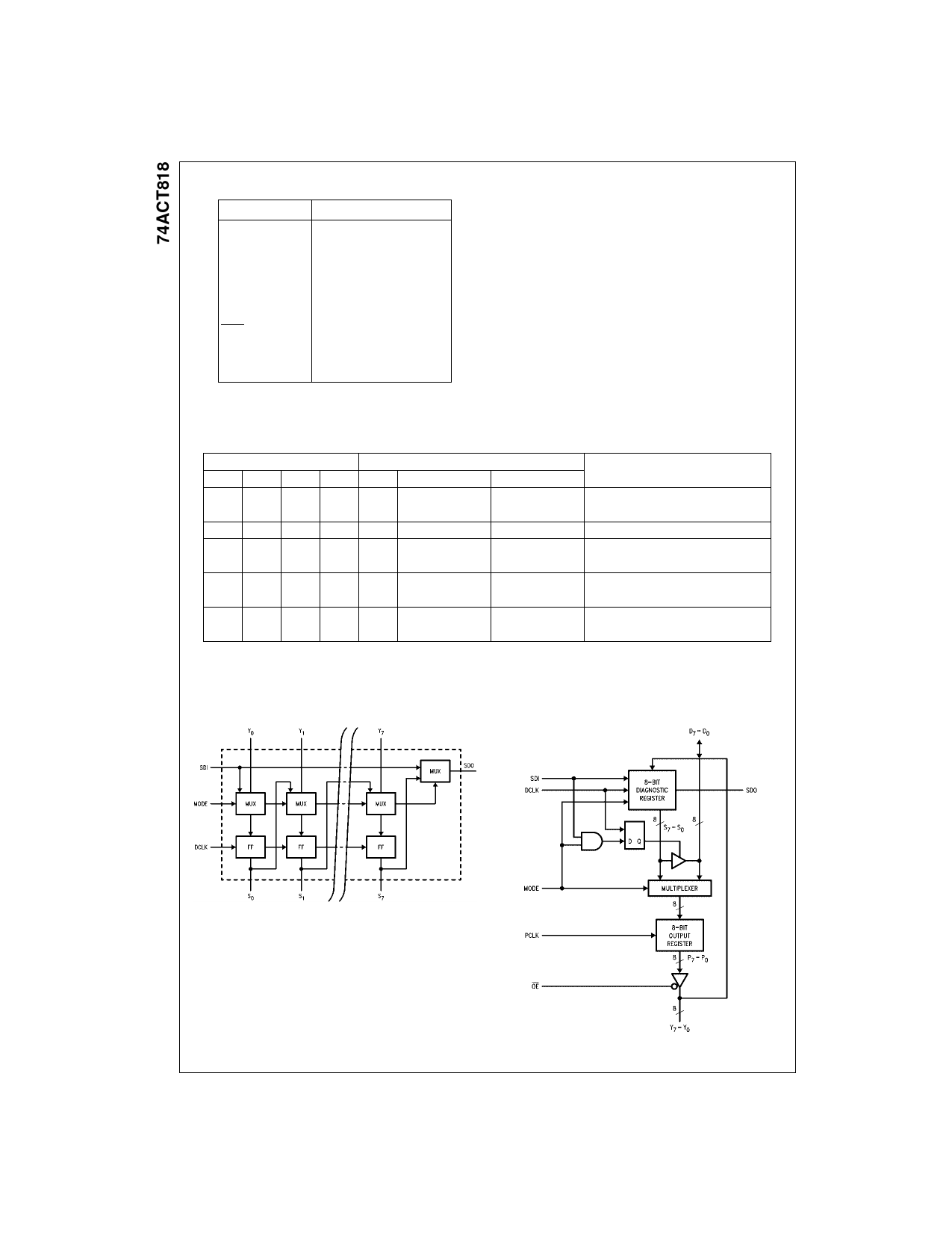
Pin Descriptions
Pin Names
D0–D7
SDI
DCLK
MODE
PCLK
OEY
SDO
Y0–Y7
Description
Data Inputs
Serial Data Input
Diagnostics Clock
Control Input
Pipeline Register Clock
Output Enable Input
Serial Data Output
Data Outputs
Functional Description
Data transfers into the diagnostic register occur on the
LOW-to-HIGH transition of DCLK. Mode and SDI deter-
mine what data source will be loaded. The pipeline register
is loaded on the LOW-to-HIGH transition of PCLK. Mode
selects whether the data source is the data input or the
diagnostic register output. Because of the independence of
the clock inputs, data can be shifted in the diagnostic regis-
ter via DCLK and loaded into the pipeline register from the
data input via PCLK simultaneously, as long as no setup or
hold times are violated. This simultaneous operation is
legal.
Function Table
Inputs
Outputs
SDI MODE DCLK PCLK SDO Diagnostic Reg. Pipeline Reg.
X
L
X
S7
SI<SI − 1,
NA
X
L
L
H
X
X
S7
L
SO<SDI
NA
SI<YI
PI<DI
NA
X
H
X
SDI
NA
PI<SI
H
H
X
H
Hold
NA
H = HIGH Voltage Level
L = LOW Voltage Level
X = Immaterial
= LOW-to-HIGH Clock Transition
Operation
Serial Shift; D7–D0 Disabled
Normal Load Pipeline Register
Load Diagnostic Register from Y;
DI Disabled
Load Pipeline Register from
Diagnostic Register
Hold Diagnostic Register; DI
Enabled
Diagnostic Register
Block Diagram
www.fairchildsemi.com
2
Share Link: 