P4C168 Просмотр технического описания (PDF) - Semiconductor Corporation
Номер в каталоге
Компоненты Описание
Список матч
P4C168 Datasheet PDF : 15 Pages
| |||
P4C168, P4C169, P4C170
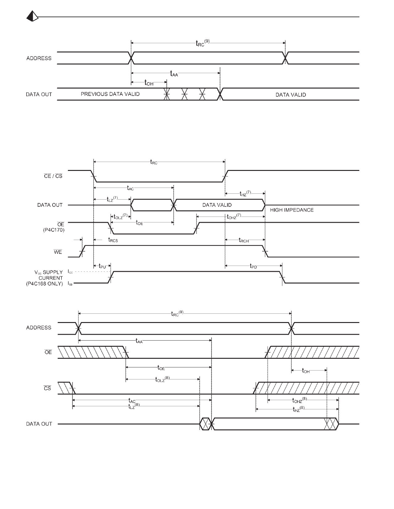
TIMING WAVEFORM OF READ CYCLE NO. 1 (ADDRESS CONTROLLED)(5,6)
Notes:
5. WE is HIGH for READ cycle.
6. CE/CS and OE are LOW for READ cycle.
TIMING WAVEFORM OF READ CYCLE NO. 2 (CE/CS CONTROLLED)(5,7)
TIMING WAVEFORM OF READ CYCLE NO. 3—P4C170 ONLY (OE CONTROLLED)(5)
Notes:
7. ADDRESS must be valid prior to, or coincident with CE/CS transition
low. For Fast CS, tAA must still be met.
8. Transition is measured ±200mV from steady state voltage prior to
change, with loading as specified in Figure 1.
9. Read Cycle Time is measured from the last valid address to the first
transitioning address.
Document # SRAM107 REV A
Page 4 of 15
Share Link: 