P4C150-20CM Просмотр технического описания (PDF) - Semiconductor Corporation
Номер в каталоге
Компоненты Описание
Список матч
P4C150-20CM Datasheet PDF : 11 Pages
| |||
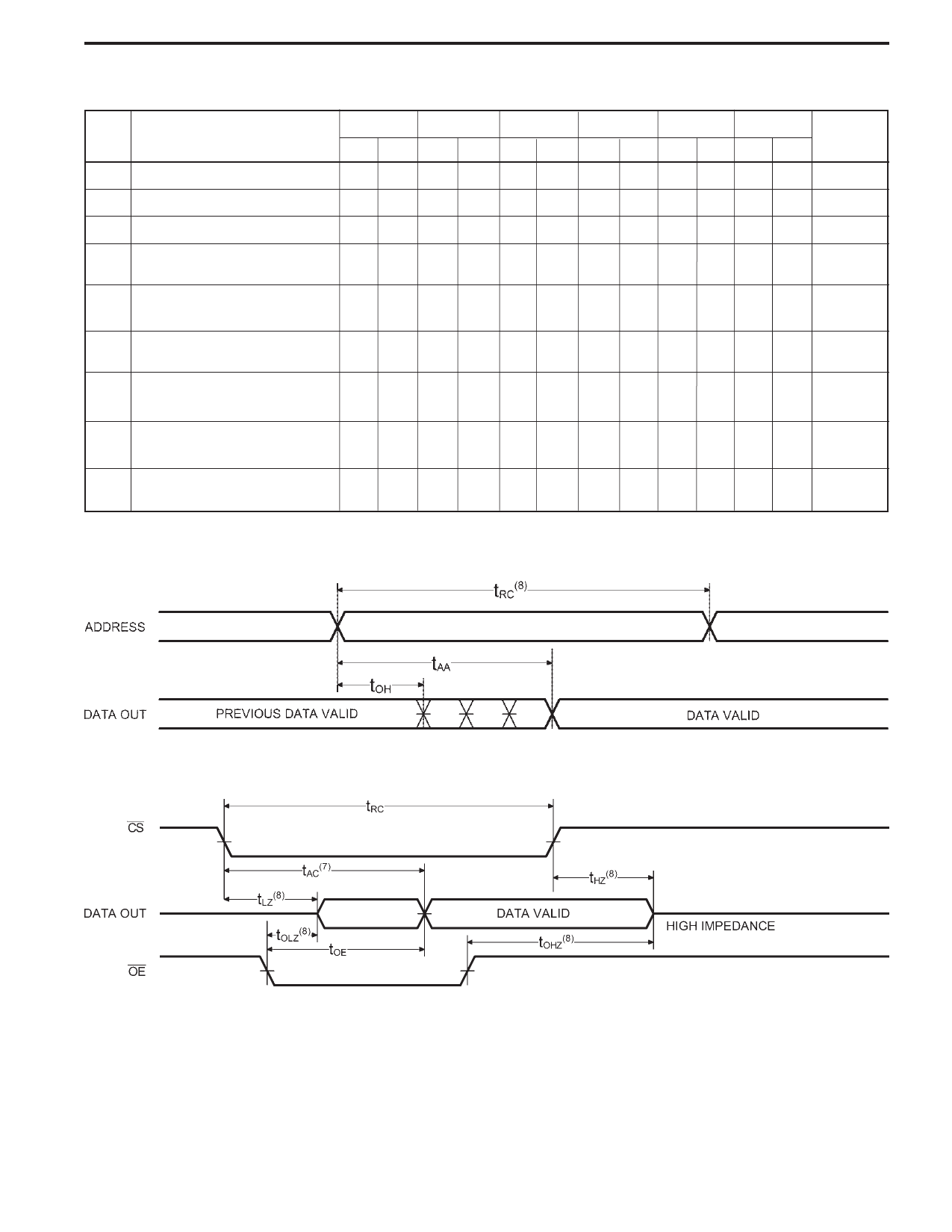
AC CHARACTERISTICS—READ CYCLE
(VCC = 5V ± 10%, All Temperature Ranges)(2)
Sym.
Parameter
tRC Read Cycle Time
tAA Address Access Time
tAC Chip Select Access Time
tOH
Output Hold from
Address Change
-10
-12
-15
-20
-25
-35
Min Max Min Max Min Max Min Max Min Max Min Max
10
12
15
20
25
35
10
12
15
20
25
35
8
10
12
14
15
35
2
2
2
2
2
2
tLZ
Chip Enable to
Output in Low Z
tHZ
Chip Disable to
Output in High Z
2
2
2
2
2
2
4
6
8
10
13
15
tOE
Output Enable to
Data Valid
7
9
10
14
15
20
tOLZ
Output Enable to
Output in Low Z
2
2
2
2
2
2
tOHZ
Output Disable to
Output in High Z
5
7
9
11
13
16
P4C150
Unit
ns
ns
ns
ns
ns
ns
ns
ns
ns
TIMING WAVEFORM OF READ CYCLE NO. 1(5,6)
TIMING WAVEFORM OF READ CYCLE NO. 2 (CS CONTROLLED)(5,7)
Notes:
5.WE is HIGH for READ cycle.
6.CS and OE are LOW for READ cycle.
7.ADDRESS must be valid prior to, or concident with, CS transition
LOW, tAA must still be met.
Document # SRAM105 REV A
8. Transition is measured ±200 mV from steady state voltage
prior to change, with loading as specified in Figure 1.
9. Read Cycle Time is measured from the last valid address to
the first transitioning address.
Page 3 of 11
Share Link: 